

Method for producing multilayer structure, multilayer structure and electronic device
A technology of lamination structure and manufacturing method, which is applied to lamination devices, lamination, electronic equipment, etc., can solve problems such as prolonged time and temperature rise, and achieve the effect of inhibiting peeling
Inactive Publication Date: 2015-03-04
SONY CORP
View PDF1 Cites 9 Cited by
- Summary
- Abstract
- Description
- Claims
- Application Information
AI Technical Summary
Problems solved by technology
Method used
View moreImage
Smart ImageViewing Examples


Examples
no. 1 approach
[0074] 1. First Embodiment (Laminated Structure and Manufacturing Method Thereof)
[0075] 2. Second Embodiment (Laminated Structure and Manufacturing Method Thereof)
no. 3 approach
[0076] 3. Third Embodiment (Laminated Structure and Manufacturing Method Thereof)
no. 4 approach
[0077] 4. Fourth Embodiment (Laminated Structure and Manufacturing Method Thereof)
Login to View More PUM
| Property | Measurement | Unit |
|---|---|---|
| thickness | aaaaa | aaaaa |
| thickness | aaaaa | aaaaa |
| width | aaaaa | aaaaa |
Abstract
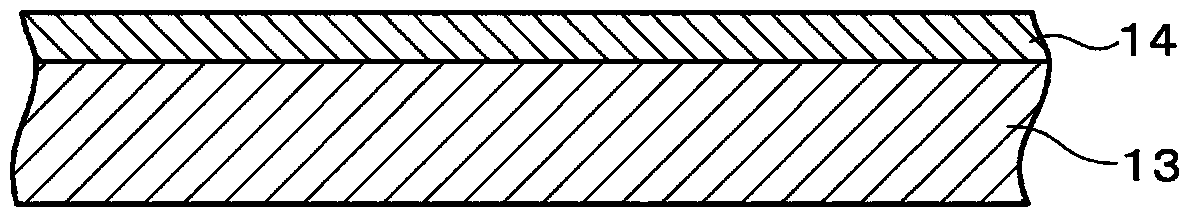
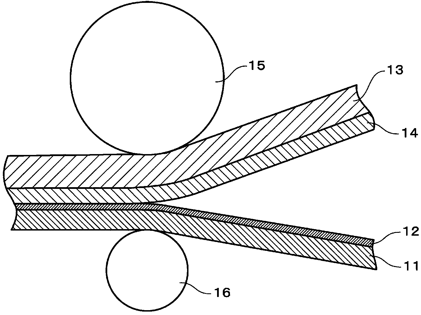
A multilayer structure is produced by bonding one or more graphene layers (12), which are formed on a first substrate (11), and a second substrate (13) with each other by a roll-to-roll method by means of an adhesive layer (14) that is formed of a delayed ultraviolet-curable resin. A metal foil is used as the first substrate (11), while a transparent substrate is used as the second substrate (13).
Description
technical field [0001] The present disclosure relates to a manufacturing method of a laminated structure, a laminated structure, and an electronic device, and is preferably applied to, for example, transparent conductive films used in displays and touch panels, and various electronic devices respectively including the transparent conductive films. Background technique [0002] Graphene including carbon atoms of single-layer graphite is expected as a transparent conductive material or a wiring material due to its high conductivity. In particular, graphene synthesized by a thermal CVD method attracts attention because a film can be formed over a large area while controlling the number of layers. [0003] In the synthesis method of graphene by thermal CVD method, graphene is formed on a metal catalyst substrate, usually on a copper foil. Therefore, the formed graphene needs to be transferred from the metal catalyst substrate to the desired substrate. [0004] As a transfer me...
Claims
Login to View More Application Information
Patent Timeline
 Patent Type & AuthorityApplications(China)
IPC IPC(8): B32B37/20B32B7/04B32B9/00G06F3/041H01B5/14H01B13/00
CPCB32B9/00B32B37/12G06F3/041B32B2311/00B32B2307/412B32B2313/04B32B7/04B32B37/20B32B2457/20B32B2457/208B32B9/007B32B9/045B32B15/08B32B15/20B32B27/16B32B2255/10Y10T428/30B32B7/12B32B2255/20B32B2255/28B32B2307/202B32B2457/00B32B37/0053B32B37/025B32B38/0008B32B38/10B32B2037/1253B32B2038/0076B32B2250/02B32B2310/0831H01B1/18
Inventor清水圭辅木村望
OwnerSONY CORP