

Vertical LED structure and manufacturing method thereof
A technology of LED structure and manufacturing method, which is applied to electrical components, circuits, semiconductor devices, etc., can solve problems such as increasing production costs and increasing LED chip production costs, and achieves solutions to heat dissipation problems, brightness enhancement problems, and production costs. Effect
- Summary
- Abstract
- Description
- Claims
- Application Information
AI Technical Summary
Problems solved by technology
Method used
Image

Examples
Embodiment Construction
[0042]Various exemplary embodiments of the present invention will now be described in detail with reference to the accompanying drawings.
[0043] Such as Figure 15 As shown, the vertical LED structure manufacturing method of the present invention comprises the following steps:
[0044] S1: providing a substrate;
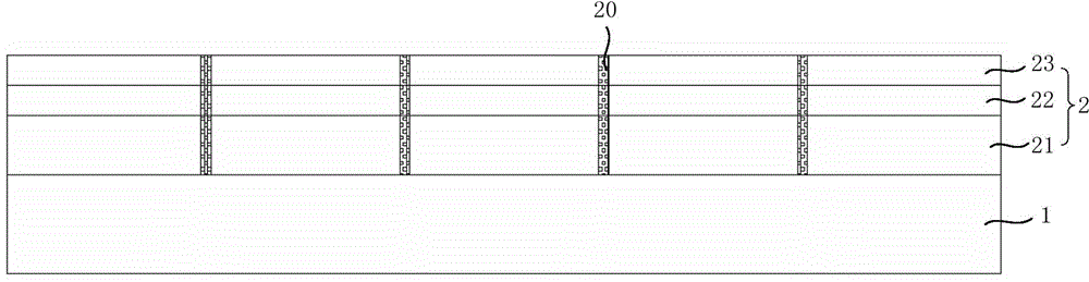
[0045] S2: forming a light-emitting semiconductor layer on the substrate, and forming several high-resistance ion implantation layers at predetermined positions of the light-emitting semiconductor layer through an ion implantation process, and the several high-resistance ion implantation layers divide the light-emitting semiconductor layer Form a number of independent light-emitting semiconductor layers that are insulated and separated, and each independent light-emitting semiconductor layer includes an N-type semiconductor layer, an active layer, and a P-type semiconductor layer stacked in sequence;
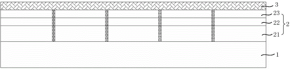
[0046] S3: forming an independent contact layer on the P-type...
PUM
 Abstract
Description
Claims
Application Information