Making method of substrate with support

A manufacturing method and technology for supporting boards, which are applied in printed circuit manufacturing, cooling/ventilating/heating transformation, mechanical/acoustic circuit processing, etc. Reduces damage and strengthens the edge area of ​​the substrate

Inactive Publication Date: 2015-03-11
NANTONG FUJITSU MICROELECTRONICS
View PDF6 Cites 3 Cited by
  • Summary
  • Abstract
  • Description
  • Claims
  • Application Information

AI Technical Summary

Problems solved by technology

[0003] However, the thinning of the substrate will increase the probability of problems such as warping and edge damage of the substrate during the packaging process.
The warping and damage of the substrate will bring inconvenience and risk to the subsequent packaging process, which will affect the product yield

Method used


Image

  • Making method of substrate with support
  • Making method of substrate with support
  • Making method of substrate with support

Examples


Embodiment Construction

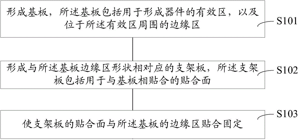
[0037] The existing substrate is prone to warping and deformation, so in the prior art, a whole board is installed on the back of the substrate. However, this kind of whole board does not protect the substrate enough, and it will easily cause the substrate to warp and deform because this kind of whole board is likely to cause uneven heating of the substrate and aggravate the deformation of the substrate, and the whole board needs to be removed after use, and the removal process is easy cause damage to the substrate.

[0038] Therefore, the present invention provides a method for manufacturing a substrate with a bracket, so as to minimize the occurrence of warpage and damage of the substrate.

[0039] In order to make the above objects, features and advantages of the present invention more comprehensible, specific embodiments of the present invention will be described in detail below in conjunction with the accompanying drawings.

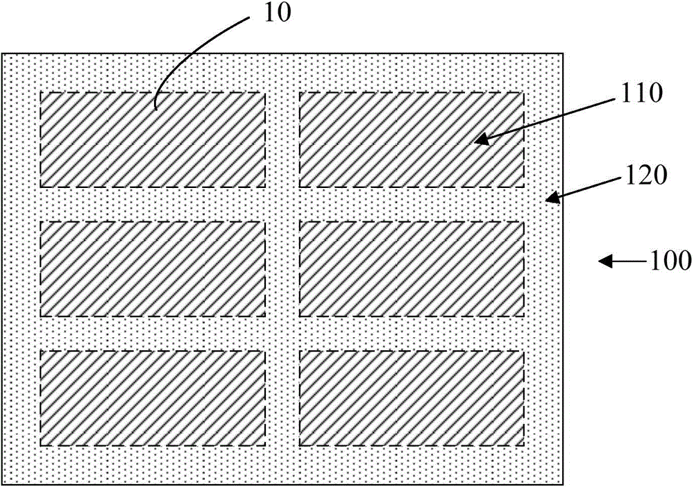
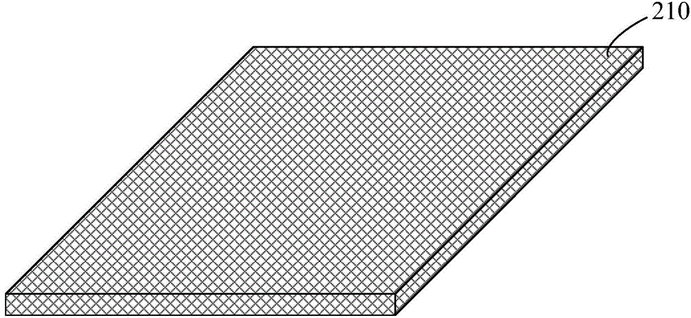
[0040] refer to figure 1 , is a schematic fl...


PUM


Abstract

The invention provides a making method of a substrate with a support. The making method comprises the following steps: forming the substrate, wherein the substrate comprises an effective zone for forming a device and an edge zone positioned at the periphery of the effective zone; forming a support plate in a shape corresponding to that of the edge zone of the substrate, wherein the support plate comprises a binding face matched with the substrate; binding and fixing the binding face of the support plate with the edge zone of the substrate. The making method has the benefits that the support plate is bonded with the substrate, so that the support plate has a function of reinforcing the edge of the substrate, and accordingly, can prevent the substrate from warping to a certain extent; the support plate and the substrate are bonded with one another and do not need to be disassembled. Compared with the mode of disassembling the bracket in the prior art, the making method can reduce the possibility that the substrate is damaged and broken.

Description

technical field [0001] The invention relates to the field of semiconductor packaging, in particular to a method for manufacturing a substrate with a bracket. Background technique [0002] With the continuous development of integrated circuit technology, electronic products are increasingly developing in the direction of miniaturization, intelligence, high performance and high reliability. The integrated circuit packaging not only directly affects the performance of integrated circuits, electronic modules and even the whole machine, but also restricts the miniaturization, low cost and reliability of the entire electronic system. With the gradual reduction of the size of the integrated circuit chip and the continuous improvement of the integration level, the electronic industry has put forward higher and higher requirements for the integrated circuit packaging technology. These requirements lead to thinner and thinner packaging substrates. [0003] However, the thinner subst...

Claims


Application Information

Patent Timeline
Patent Type & Authority Applications(China)
IPC IPC(8): H05K3/00H05K7/20
CPCH05K3/0044H05K2203/02
Inventor 朱海青
Owner NANTONG FUJITSU MICROELECTRONICS
Why Eureka
Try Eureka