
Photomask manufacturing method, photomask inspecting method, photomask inspecting apparatus, and drawing device

A manufacturing method and a technology of a drawing device, which are applied in the field of photomasks and can solve the problems of insufficient flatness of the table, deflection of the substrate, and uniform shape of the film surface.

Active Publication Date: 2015-03-18
HOYA CORP
View PDF8 Cites 4 Cited by
  • Summary
  • Abstract
  • Description
  • Claims
  • Application Information

AI Technical Summary

Problems solved by technology

[0009] (1) Insufficient flatness of the workbench,
[0010] (2) The deflection of the substrate caused by the inclusion of foreign matter on the workbench,
However, since each mask is different, it is difficult to make the surface flatness of all the perfect planes, and it is also difficult to make the film surface shape completely uniform among multiple photomasks

Method used


Image

  • Photomask manufacturing method, photomask inspecting method, photomask inspecting apparatus, and drawing device
  • Photomask manufacturing method, photomask inspecting method, photomask inspecting apparatus, and drawing device
  • Photomask manufacturing method, photomask inspecting method, photomask inspecting apparatus, and drawing device

Examples


Embodiment approach 1

[0116] The manufacturing method of the photomask of this invention has the following process.

[0117] Preparation of Photomask Blanks

[0118] In the present invention, drawing for forming a photomask based on a pattern designed based on a desired device is performed on a photomask blank formed on a main surface of a substrate. One or more thin films, and photoresist films are obtained. Therefore, a photomask blank in which the above-mentioned thin film and photoresist film were formed on one main surface of the substrate was prepared.

[0119] As the photomask blank to be prepared, a known photomask blank can be used.

[0120] As the substrate, a transparent substrate such as quartz glass can be used. Although the size and thickness are not limited, as the substrate used in the manufacture of a device for a display device, a substrate having a side of 300 mm to 1800 mm and a thickness of about 5 to 15 mm can be used.

[0121] In this application, in addition to the subst...

Embodiment approach 2

[0258]

[0259] As described above, according to the present invention, it is possible to obtain a photomask capable of extremely high coordinate accuracy of a pattern formed on a workpiece.

[0260] In addition, when such a photomask is inspected before shipment, it is most desirable to inspect in consideration of the difference between the photomask placed on the inspection device and the photomask held on the exposure device.

[0261] Therefore, the inventors found the necessity of a new inspection method.

[0262] VII Process of Obtaining Pattern Coordinate Data L

[0263] The patterned photomask was placed on the table of the coordinate inspection apparatus so that the film surface (pattern formation surface) was on the upper side, and coordinate measurement was performed. The data obtained here are assumed to be pattern coordinate data L.

[0264] Here, it is preferable to perform coordinate measurement by measuring the coordinates of the mark pattern previously form...

Embodiment

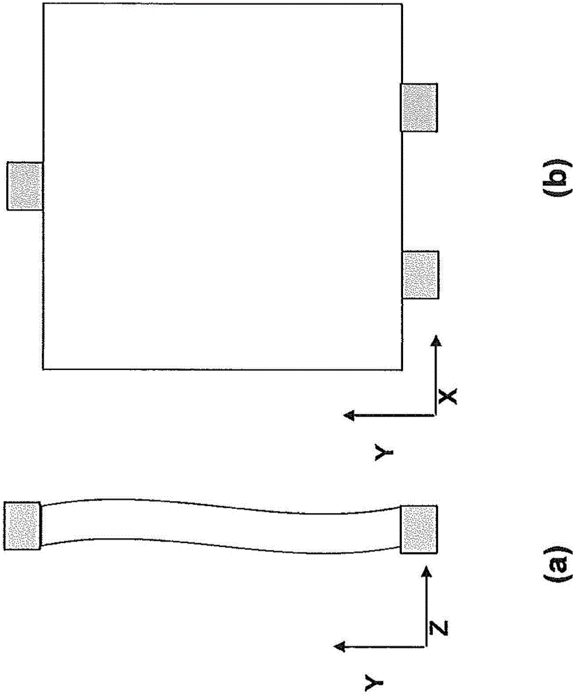
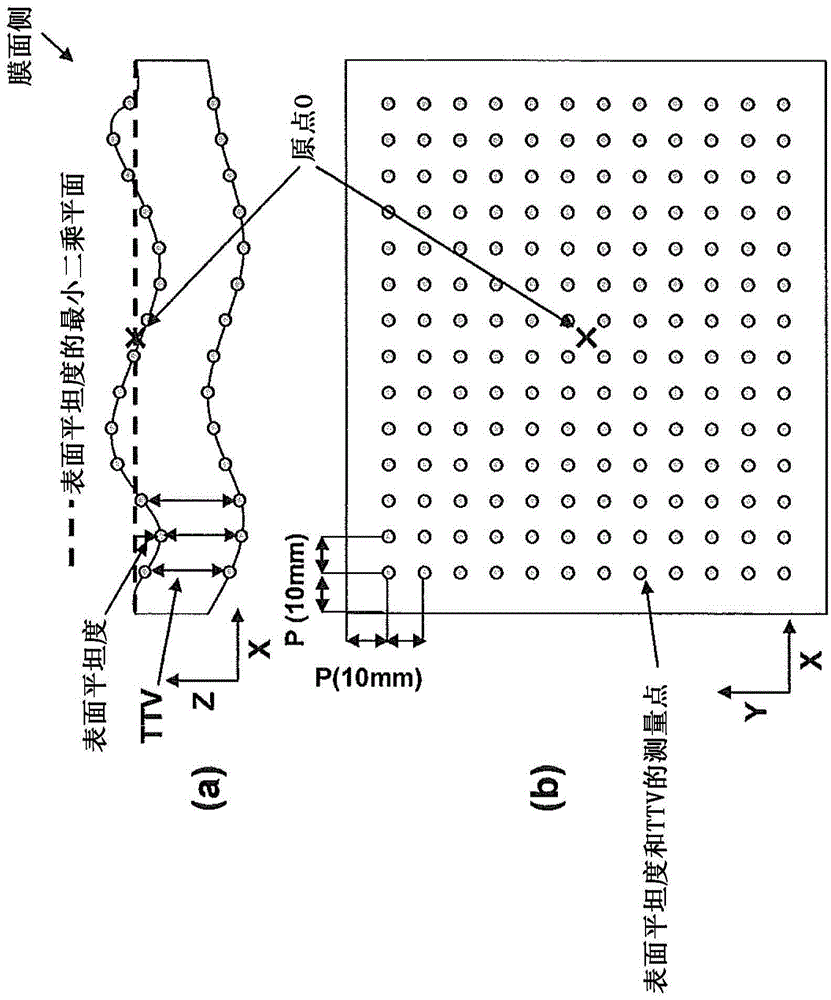
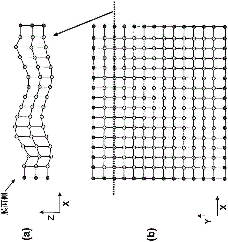
[0305] use Figure 12 The schematic diagram shown shows the effect of the invention based on the photomask manufacturing method (drawing process) of the present invention.

[0306] Here, the result obtained by simulation is shown in the case where a pattern for transfer is drawn on a substrate (photomask blank) having a specific substrate surface shape (substrate surface shape data B), where How does the coordinate accuracy of the transfer pattern change when it reaches the inside of the exposure device (as a result, how does the coordinate accuracy of the pattern formed on the transfer target change).

[0307]First, a specific test pattern was drawn on the above-mentioned photomask blank using a drawing device. In the test photomask blank used here, a light-shielding film and a positive photoresist film were formed on the main surface of a quartz substrate having a size of 800 mm×920 mm.

[0308] As the pattern design data used here, a test pattern including a cross pattern...


PUM


Abstract

The invention provides a photomask manufacturing method, a photomask inspection method, a photomask inspection apparatus, and a drawing device, which are capable of improving the coordinate precision of a pattern formed on a transferred body. The photomask manufacturing method according to the invention comprises the steps of: preparing pattern design data (A); obtaining transferred face correction data (D) representing the deformation of a main surface due to the maintaining of a photomask to an exposure apparatus and the deformation other than the dead weight deflection component; obtaining height distribution data (E) in the drawing which represent the height distribution of the main surface under such a state that the photomask green body is loaded to a work table of the drawing device; obtaining drawing differential data through the difference between the height distribution data (E) in the drawing and the transferred face correction data (D); calculating a coordinate deviation value corresponding to the drawing differential data (F), and determining coordinate deviation value data (G) for drawing; and using the coordinate deviation value data (G) for drawing and the pattern design data (A) for a drawing process on the photomask green body.

Description

technical field [0001] The present invention relates to a photomask used in the manufacture of semiconductor devices and display devices (LCD, organic EL, etc.), and to a manufacturing method and device thereof, and an inspection method and device. Background technique [0002] It is desired to improve the precision of the transfer pattern formed on the photomask, and further improve the inspection precision of the formed transfer pattern. [0003] Patent Document 1 (Japanese Unexamined Patent Application Publication No. 2010-134433) describes a drawing method and a drawing apparatus capable of improving the coordinate accuracy when transferring a photomask pattern onto a transfer target body. In particular, in the photomask manufacturing process, since the shape of the film surface (pattern formation surface) when drawing the transfer pattern is different from that at the time of exposure, it is impossible to form the designed pattern on the transfer object. Question, desc...

Claims


Application Information

Patent Timeline
IPC IPC(8): G03F1/00G03F1/84
CPCG03F1/76G03F1/84G03F1/68H01L21/027
Inventor 剑持大介
Owner HOYA CORP
Learn More