Fin manufacturing method

A manufacturing method and technology of fins, applied in semiconductor devices, electrical components, circuits, etc., can solve problems such as fins are fragile, small in size, easy to break or collapse, and achieve the effect of improving device performance and reliability

Inactive Publication Date: 2015-03-18
INST OF MICROELECTRONICS CHINESE ACAD OF SCI
View PDF12 Cites 2 Cited by
  • Summary
  • Abstract
  • Description
  • Claims
  • Application Information

AI Technical Summary

Problems solved by technology

At this point, even with well-uniform epitaxial growth, the fin size for the source/drain regions of the device is still very small, which makes it difficult to form effective contacts on these regions
On the other hand, these very small size

Method used


Image

  • Fin manufacturing method
  • Fin manufacturing method
  • Fin manufacturing method

Examples


Embodiment Construction

[0032] The features and technical effects of the technical solution of the present invention will be described in detail below with reference to the accompanying drawings and in conjunction with schematic embodiments, and a fin manufacturing method that can effectively improve the fineness of the fins and improve the insulation and isolation effect between the fins is disclosed. It should be pointed out that similar reference numerals represent similar structures, and the terms "first", "second", "upper", "lower" and the like used in this application can be used to modify various device structures or manufacturing processes . These modifications do not imply spatial, sequential or hierarchical relationships of the modified device structures or fabrication processes unless specifically stated.

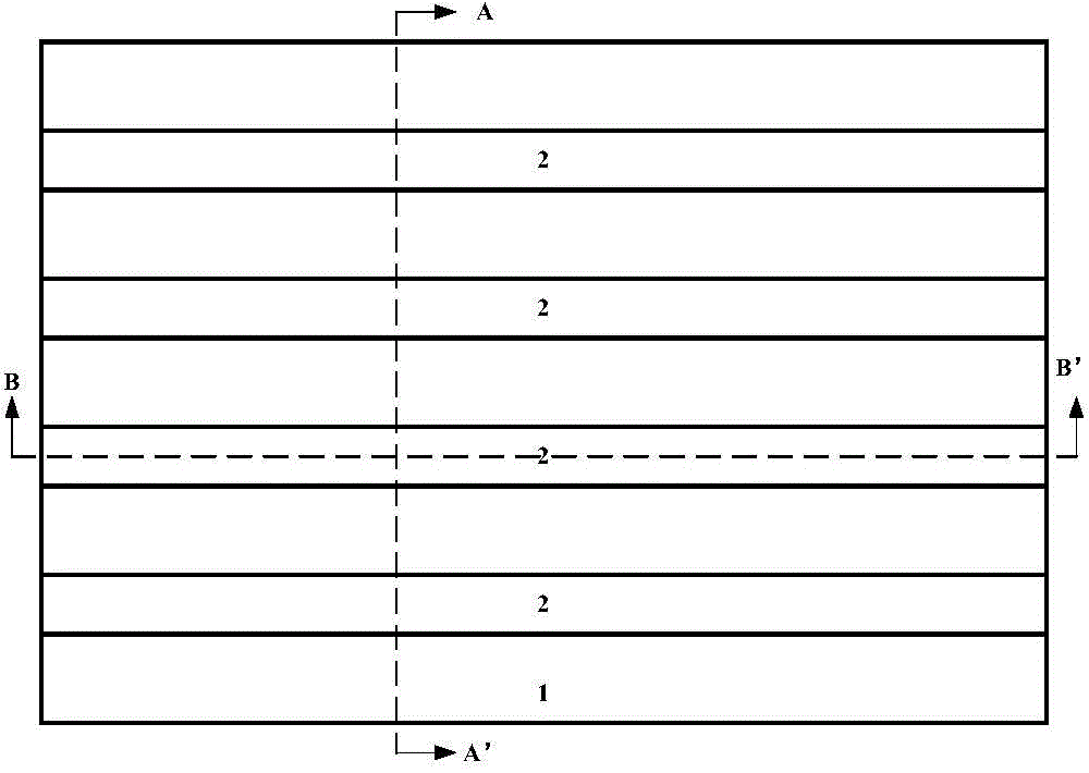
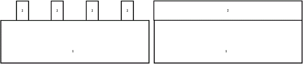
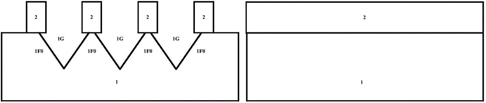
[0033] figure 1 Shown is a top view of a FinFET, tri-gate device in the prior art and the present invention, including a substrate 1 and a hard mask 2 formed on the substrate 1 . figu...


PUM


Abstract

The invention discloses a fin manufacturing method which comprises the following steps: forming multiple hard mask lines on a substrate; performing wet etching on the substrate, and forming multiple grooves and multiple initial fins among the grooves; adjusting the sectional morphology of the initial fins, reducing the top and/or bottom widths of the initial fins, and forming the final fins. According to the fin manufacturing method disclosed by the invention, refined fin lines are formed according to a special stepped etching process, and the performance and reliability of the device are improved.

Description

technical field [0001] The invention relates to a method for manufacturing a semiconductor device, in particular to a method for manufacturing fins of a FinFET device. Background technique [0002] Three-dimensional multi-gate devices such as fin field-effect transistors (FinFETs) and tri-gate (tri-gate) devices are among the most promising new device technologies as device dimensions scale down to 22nm technology and below. The control ability of the gate suppresses leakage and short channel effects. [0003] For the traditional process, the gate patterning and contact formation of CMOS devices including FinFET and tri-gate devices are performed through the following steps in order to realize isolated functional devices: [0004] 1. Using line-and-cut (line-and-cut) dual lithography patterning technology and subsequent etching of the gate stack to pattern the gate; [0005] 2. Use uniform feature size and pitch to print parallel lines for gate patterning in one direction;...

Claims


Application Information

Patent Timeline
IPC IPC(8): H01L21/28
CPCH01L29/0847
Inventor 钟汇才
Owner INST OF MICROELECTRONICS CHINESE ACAD OF SCI
Why Eureka
Try Eureka