A kind of semiconductor device and its manufacturing method

A manufacturing method and semiconductor technology, which are applied in semiconductor/solid-state device manufacturing, semiconductor devices, electric solid-state devices, etc., can solve problems such as difficulty in controlling threshold voltage variability, complex integration processes, random fluctuations of dopants, etc.

Active Publication Date: 2017-08-01
SEMICON MFG INT (SHANGHAI) CORP
View PDF6 Cites 0 Cited by
  • Summary
  • Abstract
  • Description
  • Claims
  • Application Information

AI Technical Summary

Problems solved by technology

Fin Field Effect Transistor (FinFET) has excellent electrostatic control ability due to its small device size and small operating voltage. However, the reduction of device size and operating voltage, especially the reduction of operating voltage, leads to the threshold Control of voltage variability becomes very difficult
In semiconductor devices with large-scale application of Fin Field Effect Transistors (FinFETs), as the process node continues to decrease, the number of ions that need to be implanted continues to decrease (for example, the number of ions that need to be implanted for devices using a 10nm process node is very small), The ion implantation process becomes very difficult to control
[0003] Different metal capping process (capping) can effectively adjust the threshold voltage of FinFET, but this method requires complex integration process and does not bring other improvements
However, the traditional ion implantation process will reduce the ion mobility of the device and may cause random fluctuations of dopants that have a very bad impact on the device.
Also, for the manufacturing method of semiconductor devices using metal gate technology, the ion implantation process also faces the challenge of controlling the ion implantation dose to prevent ions from penetrating into the high-k dielectric layer or the channel region of the device

Method used


Image

  • A kind of semiconductor device and its manufacturing method
  • A kind of semiconductor device and its manufacturing method
  • A kind of semiconductor device and its manufacturing method

Examples


Embodiment 1

[0100] An embodiment of the present invention provides a method for manufacturing a semiconductor device. The method realizes the adjustment of the threshold voltage of the transistor by adding a cap layer (cap layer) and a barrier layer (barrier layer) in the gate stack structure, which can be more Semiconductor devices with multiple threshold voltages are well realized.

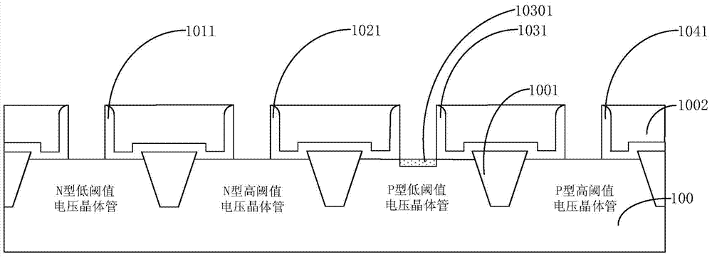
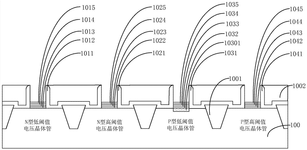
[0101] Below, refer to Figure 1A to Figure 1H as well as Figure 3A A method for manufacturing a semiconductor device proposed in Embodiment 1 of the present invention will be described. in, Figure 1A to Figure 1H A schematic cross-sectional view of a structure formed in the relevant steps of a method for manufacturing a semiconductor device according to an embodiment of the present invention; Figure 3A It is a typical flowchart of a manufacturing method of a semiconductor device according to an embodiment of the present invention.

[0102] The method for manufacturing a semiconductor device according ...

Embodiment 2

[0167] The embodiment of the present invention provides another method for manufacturing a semiconductor device, which also realizes the adjustment of the threshold voltage of the transistor by adding a cap layer (cap layer) and a barrier layer (barrier layer) in the gate stack structure, Semiconductor devices with multiple threshold voltages can be better realized. The difference from Embodiment 1 is that the manufacturing method of the semiconductor device in this embodiment omits the step of forming a silicon germanium layer in the channel region of the P-type low-voltage transistor, and adds the step of forming a fourth function in the P-type low-voltage transistor. Function metal layer steps.

[0168] Below, refer to Figure 2A to Figure 2G as well as Figure 3B A method for manufacturing a semiconductor device proposed in Embodiment 2 of the present invention will be described. in, Figure 2A to Figure 2G A schematic cross-sectional view of a structure formed in the ...

Embodiment 3

[0220] An embodiment of the present invention provides a semiconductor device, which can be manufactured by using the method for manufacturing the semiconductor device in the first embodiment above.

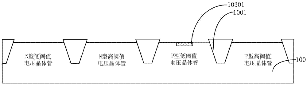
[0221] Below, refer to Figure 4 The structure of a semiconductor device proposed in Embodiment 3 of the present invention will be described. in, Figure 4 It is a schematic cross-sectional view of the structure of a semiconductor device according to an embodiment of the present invention.

[0222] Such as Figure 4 As shown, the semiconductor device of this embodiment includes: a semiconductor substrate 100 and an N-type low-threshold voltage transistor, an N-type high-threshold voltage transistor, a P-type low-threshold voltage transistor, and a P-type high-threshold voltage transistor located on the semiconductor substrate 100 . Wherein, the N-type low-threshold voltage transistor, the N-type high-threshold voltage transistor, the P-type low-threshold voltage transistor, a...


PUM


Abstract

The invention provides a semiconductor device and a preparation method thereof, relating to the technical field of semiconductors. The preparation method of the semiconductor device has the beneficial effect that regulation of threshold voltages of transistors is achieved by adding cap layers and barrier layers in a gate laminated structure, so that the semiconductor device with multiple threshold voltages can be better achieved. Regulation of the threshold voltages of the transistors can be achieved as the cap layers and the barrier layers are added in the gate laminated structure, so that the semiconductor device has better threshold voltage characteristics.

Description

technical field [0001] The invention relates to the technical field of semiconductors, in particular to a semiconductor device and a manufacturing method thereof. Background technique [0002] In the field of semiconductor technology, how to reduce power consumption while ensuring the performance of semiconductor devices has become a major challenge faced by people. Power consumption / performance optimization (Power-performance optimization) usually requires semiconductor devices to have multiple threshold voltages (Vt) and low off-current (Ioff). In planar bulk silicon semiconductor devices, multiple threshold voltages are achieved by using two work function layers (corresponding to NFET and PFET respectively) and using different gate lengths and doping concentrations. Fin Field Effect Transistor (FinFET) has excellent electrostatic control ability due to its small device size and small operating voltage. However, the reduction of device size and operating voltage, especial...

Claims


Application Information

Patent Timeline
Patent Type & Authority Patents(China)
IPC IPC(8): H01L21/8238H01L21/28H01L27/092H01L29/49
CPCH01L21/28008H01L21/823821H01L21/823857H01L27/0922H01L27/0924H01L29/513H01L29/518
Inventor 谢欣云
Owner SEMICON MFG INT (SHANGHAI) CORP
Why Eureka
Try Eureka