Wide-view surface defect detector

A defect detection, wide field of view technology, applied in the direction of optical testing flaws/defects, can solve the problems of low efficiency, small field of view, long inspection time, etc., to avoid defects, improve work efficiency, and easy to master

Inactive Publication Date: 2015-03-25
UNIONLIGHT TECH
View PDF11 Cites 6 Cited by
  • Summary
  • Abstract
  • Description
  • Claims
  • Application Information

AI Technical Summary

Problems solved by technology

[0003] The existing method is to use an optical microscope to identify defects on the surface of the wafer through the eyes, but as the demand for large-diameter wafers continues to increas

Method used


Image

  • Wide-view surface defect detector
  • Wide-view surface defect detector
  • Wide-view surface defect detector

Examples


Example Embodiment

[0025] The present invention will be further described below in conjunction with specific drawings and embodiments.

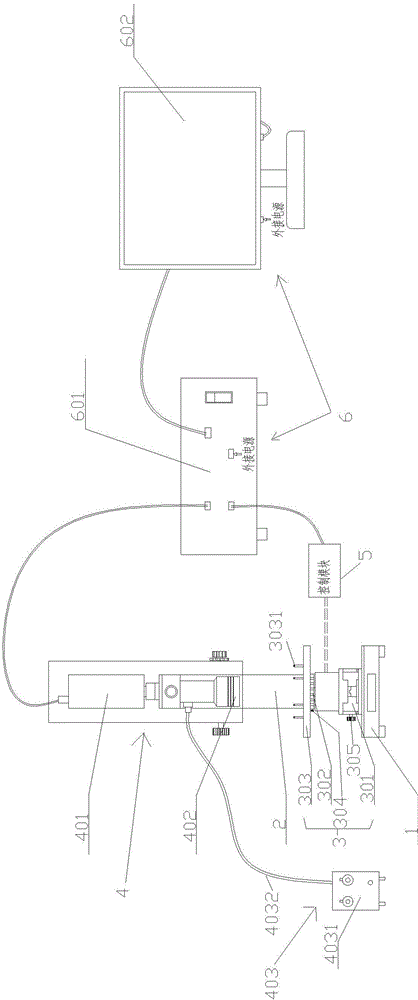
[0026] Such as figure 1 As shown, the wide-view surface defect detection device proposed by the present invention includes a base 1 and a column 2 fixed on the base 1, and also includes a bearing mechanism 3, a detection mechanism 4, a control module 5 and a computer system 6. The vertical rail 2 is provided with a vertical rail, and the detection mechanism 4 cooperates with the vertical rail on the vertical column to realize the up and down sliding of the detection mechanism.

[0027] The carrying mechanism 3 is assembled on the base 1 for carrying and holding the wafer to be inspected. The carrying mechanism 3 can move along the X axis and can drive the wafer to rotate horizontally. figure 1 In, the direction perpendicular to the paper surface is the X-axis direction, which is hereby explained. Column 3 is fixed on one side of base 1 ( figure 1 The middle is the ...


PUM


Abstract

The invention provides a wide-view surface defect detector. The wide-view surface defect detector comprises a base, a vertical column, a bearing mechanism, a detecting mechanism, a control module and a computer system, wherein the vertical column is fixed on the base; the bearing mechanism is used for bearing and clamping a wafer, is assembled on the base, can move along the X axis, and can drive the wafer to rotate horizontally; the detecting mechanism is assembled on the vertical column, can move vertically along the vertical column, can perform amplification imaging detection on the surface of the wafer on the bearing mechanism, and can transmit a detection image back; the control module is connected with the bearing mechanism, and is used for controlling the bearing mechanism to move along the X axis and driving the wafer to rotate horizontally, so that the detecting mechanism can perform the imaging detection on each part of the surface of the wafer; the computer system is used for processing the detection image transmitted back by the detecting mechanism, and recognizing wafer surface defects in the image. The wide-view surface defect detector is suitable for the surface detection of the heavy-caliber wafers, is high in detection speed, and is high in efficiency.

Description

technical field [0001] The invention relates to an optical detection device, in particular to a detection device for detecting wafer surface defects. Background technique [0002] For semiconductor optoelectronic devices, wafer surface defects are an important factor affecting the performance of optoelectronic devices. The focus of the wafer surface is the nano-level surface roughness and the flaws that cannot be observed on the nano-level surface. The main surface defects include scratches and cracks. , dirt, air bubbles, fingerprints and more. In order to ensure the performance of optoelectronic devices, wafer manufacturers need to perform a comprehensive inspection of the surface of the wafer. [0003] The existing method is to use an optical microscope to identify defects on the surface of the wafer through the eyes, but as the demand for large-diameter wafers continues to increase, from 2 inches to 4 inches, and even to 6 inches and 8 inches, the existing microscope in...

Claims


Application Information

Patent Timeline
IPC IPC(8): G01N21/95
Inventor 王联欧阳志刚裴广庆刘广月
Owner UNIONLIGHT TECH
Why Eureka
Try Eureka