Array substrate, manufacturing method of array substrate and display device

An array substrate and substrate technology, applied in the field of display devices, can solve problems such as the decrease of electron mobility of thin film transistors and affect the performance of thin film transistors, and achieve the effect of reducing performance differences

Active Publication Date: 2015-03-25
BOE TECH GRP CO LTD +1
View PDF6 Cites 11 Cited by
  • Summary
  • Abstract
  • Description
  • Claims
  • Application Information

AI Technical Summary

Problems solved by technology

In the case of forming grain boundaries, if there is an angle between the channel current direction of the thin film transistor formed on the polysilicon thin film layer and the extension direction of the grain boundary, the electron mobility of the thin film transistor will decrease, thereby affecting the performance of the thin film transistor

Method used


Image

  • Array substrate, manufacturing method of array substrate and display device
  • Array substrate, manufacturing method of array substrate and display device
  • Array substrate, manufacturing method of array substrate and display device

Examples


Embodiment Construction

[0034]The technical solutions of the present invention will be further specifically described below through the embodiments and in conjunction with the accompanying drawings. In the specification, the same or similar reference numerals designate the same or similar components. The following description of the embodiments of the present invention with reference to the accompanying drawings is intended to explain the general inventive concept of the present invention, but should not be construed as a limitation of the present invention.

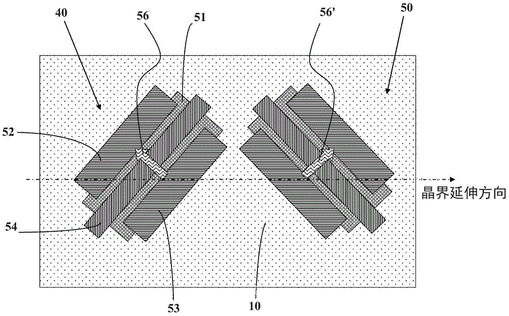
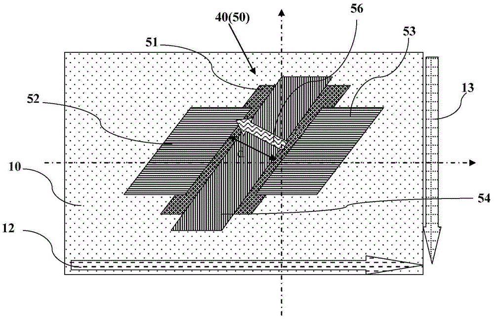
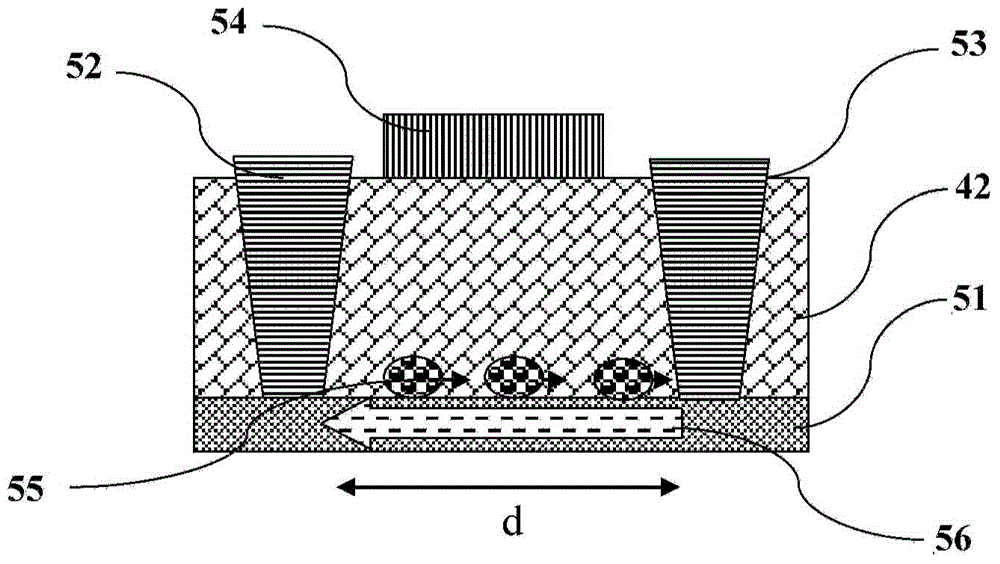
[0035] According to the general inventive concept of various exemplary embodiments of the present invention, there is provided an array substrate including: a substrate; a polysilicon thin film including a plurality of grain boundaries extending in the same direction; and at least one channel A thin film transistor whose current direction is the first direction, and at least one thin film transistor whose channel current direction is the second...


PUM


Abstract

The invention discloses an array substrate, a manufacturing method of the array substrate and a display device. The array substrate comprises a substrate body, a poly-Si thin film and multiple thin film transistors. The poly-Si thin film comprises multiple crystal boundaries extending in the same direction. The multiple thin film transistors comprise at least one thin film transistor with the channel current direction as the first direction and at least one thin film transistor with the channel current direction as the second direction. The first direction and the second direction are different. Each thin film transistor comprises a grid electrode, an active layer, a source electrode and a drain electrode, wherein the active layer is composed of the poly-Si thin film. The included angle between the first direction and the crystal boundary extending direction and the included angle between the second direction and the crystal boundary extending direction are not equal to 90 degrees. By reducing difference of influence of the crystal boundaries on the electronic mobility of the thin film transistors with the channel current in the first direction and the thin film transistors with the channel current in the second direction, performance difference of the two kinds of thin film transistors is reduced.

Description

technical field [0001] Embodiments of the present invention relate to a display device, in particular to an array substrate based on a low-temperature polysilicon thin film transistor, a manufacturing method thereof, and a display device including the array substrate. Background technique [0002] Currently, thin film transistors (TFTs) widely used in liquid crystal display devices and AMOLED (Active Matrix Organic Light Emitting Diode, active matrix organic light emitting diode) display devices mainly include amorphous silicon thin film transistors and polycrystalline silicon thin film transistors. Among them, low temperature polysilicon (Low Temperature Poly-Silicon; LTPS) technology has also been applied to the manufacturing process of thin-film transistor displays, which mainly transforms amorphous silicon (a-Si) thin films by excimer laser annealing process (Excimer Laser Anneal) It is a polysilicon (Poly-Si) film. Electron mobility is increased by more than 100 times ...

Claims


Application Information

Patent Timeline
Patent Type & Authority Applications(China)
IPC IPC(8): H01L27/12H01L29/786H01L29/04H01L21/336H01L21/84
Inventor 莫再隆朴承翊石天雷
Owner BOE TECH GRP CO LTD
Why Eureka
Try Eureka