

Gate structure of separation gate power device and process method
A power device and gate structure technology, applied in semiconductor devices, electrical components, circuits, etc., can solve problems such as complex process, reduced product performance, deterioration, etc., to reduce diffusion effects, solve connection problems, and have no pollution problems.
- Summary
- Abstract
- Description
- Claims
- Application Information
AI Technical Summary
Problems solved by technology
Method used
Image

Examples
Embodiment Construction
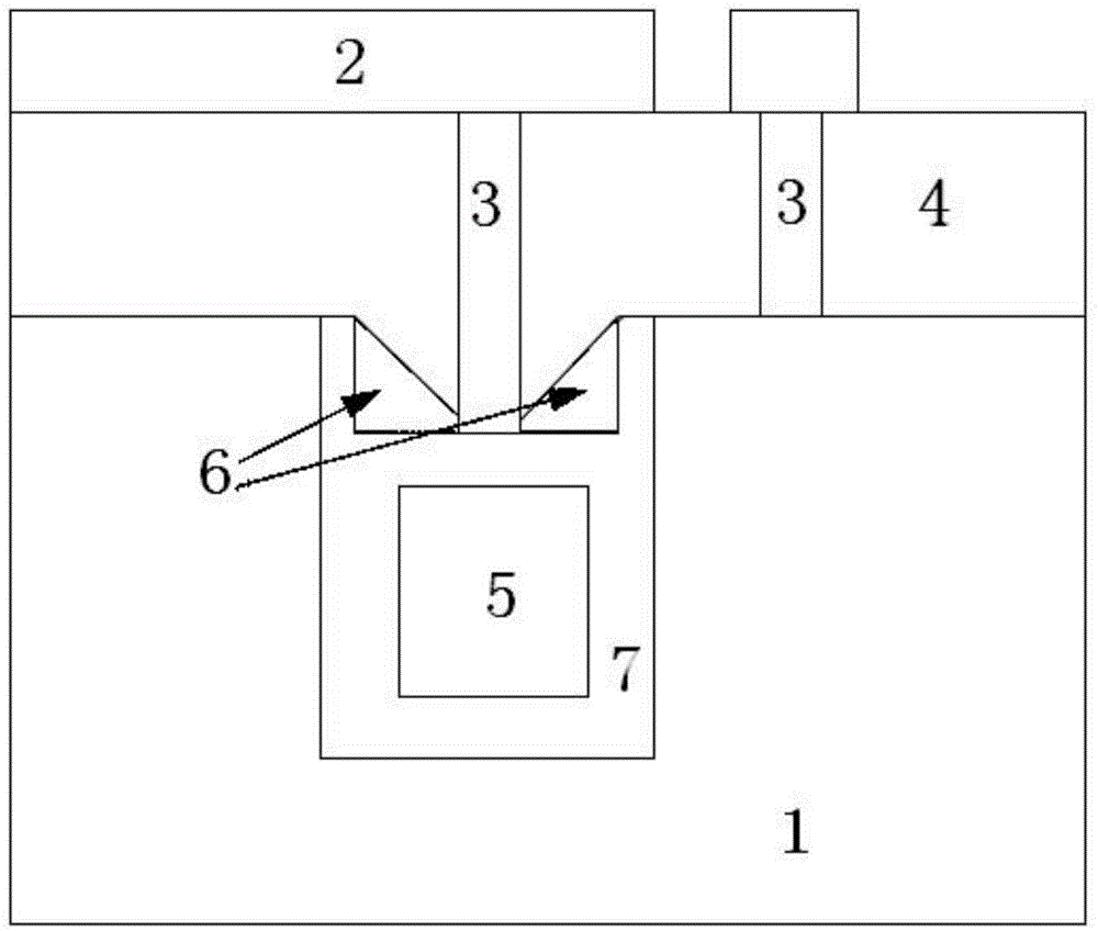
[0032] The gate structure of the split-gate power device described in the present invention, such as Figure 9 As shown, there is a trench on the silicon substrate 1, and a layer of oxide layer 7 is attached to the side wall and bottom of the trench. The lower part of the trench has a separate gate 5, and the upper part of the separate gate 5 is also covered with a layer of silicon oxide. The silicon oxide layer on the side wall of the groove and the bottom of the groove together form the separation gate, the upper part of the trench is the gate 6, the surface of the silicon substrate 1 is the interlayer dielectric, and the metal lead 2 connects the gate through the contact hole 3 passing through the interlayer dielectric 4. Pole 6 leads out. The gate 6 is a polysilicon thin gate with a U-shaped structure, and its interior is filled with metal tungsten 8 . The contact hole 3 is connected with the filled metal tungsten 8 to lead out the gate 6 .
[0033] Between the polysilico...
PUM
 Abstract
Description
Claims
Application Information