A current signal demodulation circuit
A technology for demodulating circuits and current signals, applied in the electrical field, can solve the problems of difficult circuit matching, few nodes, insufficient charging and discharging of coupling capacitors, etc., to achieve high communication rate range, reduce product cost, and reduce sampling The effect of power consumption
- Summary
- Abstract
- Description
- Claims
- Application Information
AI Technical Summary
Problems solved by technology
Method used
Image

Examples
Embodiment Construction
[0050] The present invention will be described in detail below in conjunction with the accompanying drawings, principles and specific embodiments.
[0051] Principle description:
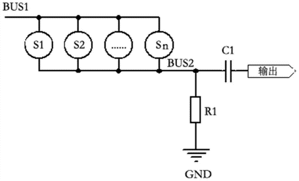
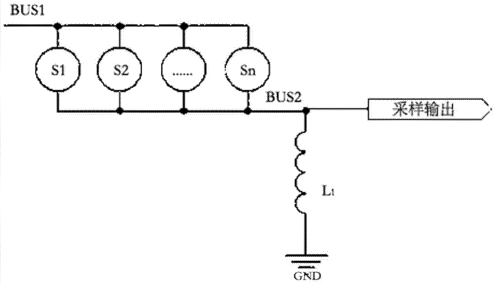
[0052] The demodulation circuit of master station of the present invention flows through slave station S1, slave station S2, ..., slave station S from bus BUS1 N The current signal arriving at the bus BUS2 is sampled by the inductance sampling circuit, and then output to the lower circuit after sampling.
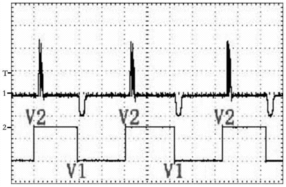
[0053] If the inductance sampling circuit uses series inductor L1 to sample, such as figure 2 shown, then one can obtain image 3 In the waveform shown, channel 1 is the sampling waveform, and channel 2 is the current waveform of the bus.
[0054] From image 3 We can see that the rising edge current signal generates a positive spike pulse group V2 on the inductor, and the falling edge current signal generates a negative spike pulse group V1 on the inductor.
[0055] Additionally, from image...
PUM
 Abstract
Description
Claims
Application Information
 - R&D
- Intellectual Property
- Life Sciences
- Materials
- Tech Scout
- Unparalleled Data Quality
- Higher Quality Content
- 60% Fewer Hallucinations
Browse by: Latest US Patents, China's latest patents, Technical Efficacy Thesaurus, Application Domain, Technology Topic, Popular Technical Reports.
© 2025 PatSnap. All rights reserved.Legal|Privacy policy|Modern Slavery Act Transparency Statement|Sitemap|About US| Contact US: help@patsnap.com