A surface plasmon slow light waveguide

A surface plasmon and optical waveguide technology, applied in the field of nanophotonics, can solve the problems of signal crosstalk and insufficient restraint, and achieve the effects of small transmission loss, easy implementation, and reduced transmission loss

Active Publication Date: 2017-06-27
GUILIN UNIV OF ELECTRONIC TECH
View PDF6 Cites 0 Cited by
  • Summary
  • Abstract
  • Description
  • Claims
  • Application Information

AI Technical Summary

Problems solved by technology

For example, a new type of slow light waveguide is to connect multiple silicon teeth with gradually increasing height on the metal substrate. Most of the field generated by the waveguide of this structure is in the middle of the silicon teeth, but there is still a large part of the field in the air above the silicon teeth. When used in nano-integrated circuits, the air field will generate signal crosstalk with other devices, and the constraints are not enough

Method used


Image

  • A surface plasmon slow light waveguide
  • A surface plasmon slow light waveguide
  • A surface plasmon slow light waveguide

Examples


Embodiment Construction

[0027] The present invention will be described in further detail below in conjunction with the accompanying drawings and embodiments.

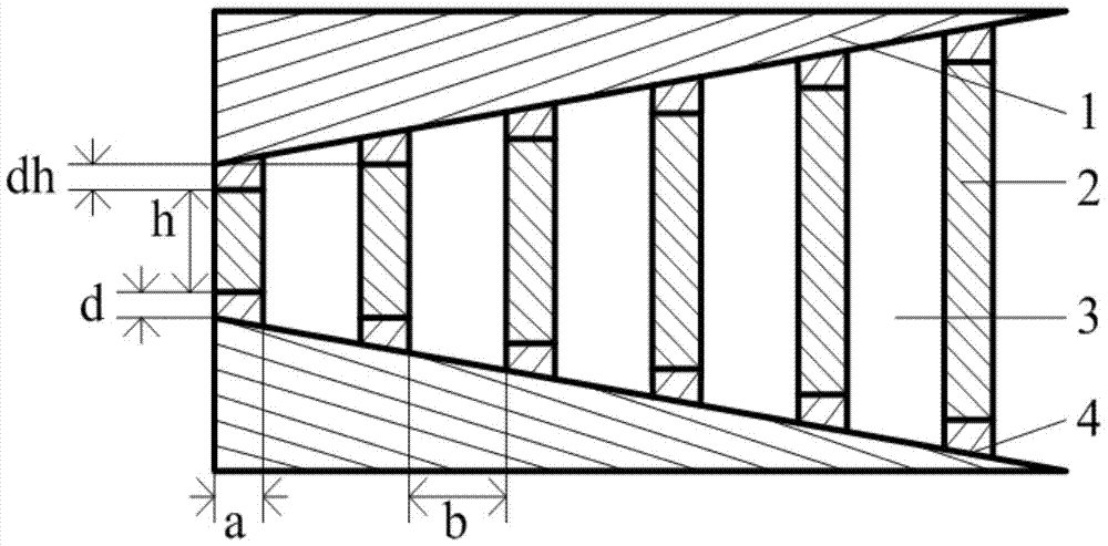
[0028] The structure of this surface plasmon slow light waveguide embodiment is as follows figure 1 As shown, the upper and lower metal bases 1 are the same right-angled triangle with opposite hypotenuses, and are symmetrical with respect to the horizontal center line. The material of the metal base 1 in this example is silver.

[0029] The upper and lower ends of the grating bars of the dielectric grating 2 are respectively connected to the upper and lower metal bases 1 through the loading medium layer 4 . The horizontal center line between the upper part of the dielectric grating 2 and the lower metal base 1 is symmetrical up and down. In this example, the material of the dielectric grating 2 is silicon with a relative permittivity of 11.9, and the material of the loading dielectric layer 4 is silicon dioxide. The relative permittivity is ...


PUM


Abstract

The invention provides a surface plasma slow light waveguide. Upper and lower metal bases are arranged; upper and lower ends of grids of a medium optical grating are connected with the upper and lower metal bases through the medium optical grating respectively. The grids of the medium optical grating are symmetrical up and down by the horizontal central line between the upper and lower metal bases; the widths a of all the grids and the distances b are equal; the height of each grid is gradually increased from one end to the other end by the same increasing extent 2dh; at least four grids are arranged. Air or vacuum is formed between the grids. Preferentially, the metal bases are made of silver and the medium optical grating is made of silicon; a loading medium layer is silicon dioxide. According to the surface plasma slow light waveguide, the transmission low of surface plasmas is greatly reduced and the surface plasma slow light waveguide has the advantages of slow transmission speed and small loss in a certain range; the medium optical grating is surrounded by the upper and lower metal bases and the field is restricted in the grids, so that the extremely strong binding character of the field is realized; meanwhile, the advantages of low loss, strong binding character and slow group velocity are realized.

Description

technical field [0001] The invention belongs to a waveguide in the field of nanophotonics, in particular to a surface plasmon slow light waveguide. Background technique [0002] Surface plasmons (SPs) are electromagnetic waves that travel along the surface of a conductor and can be generated by resonant excitation of light waves and electrons on the conductor surface. The electromagnetic wave propagates along the direction of the conductor surface, and decays exponentially in the direction perpendicular to the conductor surface, so it is bound to propagate on the conductor surface. Because surface plasmons can overcome the diffraction limit, they are considered to be a promising carrier for transmitting optical information in micro-nano devices. By selecting different shapes of conductor surface structures, different forms of surface plasmon polarization can be guided to propagate, especially Novel photonic integrated circuits at the nanometer scale have great potential and...

Claims


Application Information

Patent Timeline
Patent Type & Authority Patents(China)
IPC IPC(8): G02B6/122G02B6/124
CPCG02B6/122G02B6/124
Inventor 陈辉陈佳佳陈明
Owner GUILIN UNIV OF ELECTRONIC TECH
Why Eureka
Try Eureka