Polarization light guide planar waveguide optical display device

A technology of optical display and planar waveguide, which is applied in optical components, planar/plate-shaped light guides, optics, etc., can solve the problems of limited expansion of display field of view, unfavorable large-scale production of devices, and poor appearance of devices. Achieve the effect of simple and easy optical design and processing technology, high light wave coupling efficiency and compact structure

Active Publication Date: 2015-04-08
SHANGHAI RAYPAI PHOTONIC CRYSTAL LTD
View PDF9 Cites 45 Cited by
  • Summary
  • Abstract
  • Description
  • Claims
  • Application Information

AI Technical Summary

Problems solved by technology

The disadvantage of this scheme is that due to the use of large-angle S light reflection and small-angle P light transmission, the projected area of ​​the reflection output surface on the bottom surface of the substrate is too small, which is not conducive to the expansion of the field of view, and at the same time increases the difficulty of design. The thickness of the device cannot be reduced
U.S. Patent US20100260455 uses a micro-sawtooth structure to expand the display field of view of the display device, but the overall thickness of the device is not reduced, and the overall appearance of the device is not good enough to bring comfort to the we...

Method used


Image

  • Polarization light guide planar waveguide optical display device
  • Polarization light guide planar waveguide optical display device
  • Polarization light guide planar waveguide optical display device

Examples


Embodiment Construction

[0026] The specific working process of the present invention will be described below with reference to the accompanying drawings.

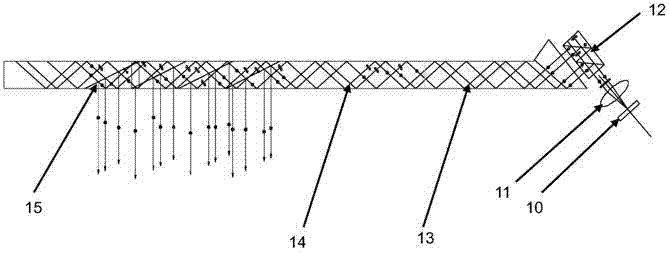
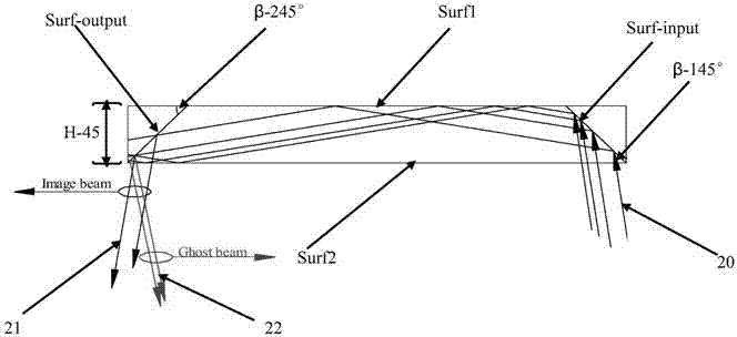
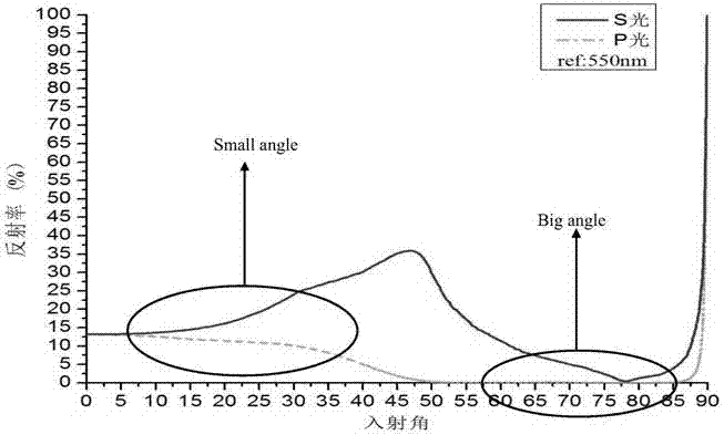
[0027] figure 1 It is a schematic diagram of the planar waveguide optical display device for polarized light guide according to the present invention. like figure 1 As shown, the system composition of the present invention includes: an image display light source 10, a collimating lens group 11, a PBS polarization beam splitting prism group 12, a plane light guide transmission substrate 13, a polarization conversion light guide substrate 14 and a small-angle coupling output surface 15 . The light from the image display light source 10 is collimated by the lens group 11 and then enters the PBS polarization beam splitting prism group 12 . The polarization beam splitting group selectively refracts the incoming P light and S light, so that the P light is completely transmitted without loss as much as possible, and the S light is completely reflected...


PUM


Abstract

The invention provides a polarization light guide planar waveguide optical display device which comprises an image display light source, a collimating lens assembly, a PBS (poly butylene succinate) polarization beam splitter assembly, a planar light guide transmission substrate, a polarization conversion light guide substrate and a small-angle coupling output surface. The image display light source is used for emitting a display light wave for displaying a needed image, the collimating lens assembly is used for collimating light waves emitted by the light source, the PBS polarization beam splitter assembly is used for correspondingly splitting the light waves, the planar light guide transmission substrate is used for performing reflection propagation for coupled-into light waves to form total-reflection light waves, the polarization conversion light guide substrate is used for converting polarization states of the light waves, and the small-angle coupling output surface is mainly used for coupling the light waves out of the substrate and enlarging viewing fields. The polarization light guide planar waveguide optical display device has the advantages that the device is compact in structure, light and large in viewing field, an optical design and machining process is simple and easy to implement, and the device can be used for the fields such as wearing display, 3D (three-dimensional) naked eye display, automobile navigation and wild map instruction.

Description

technical field [0001] The present invention relates to an optical display device, in particular to a planar waveguide optical display device that can be used for polarized light guide for whole-eye augmented reality. Background technique [0002] For the head-mounted display optical system, in order to reflect the effect of augmented reality, optical components are usually used to virtually display image information at a certain distance in front of the human eyes, so that the wearer can observe the surrounding scenery while browsing the information. changes so as not to affect normal behavior. Therefore, in order to enable the wearer to obtain all the information from the display light source in time, the augmented reality wearable display optical system usually requires the display system to have a large field of view, a light and thin structure, and uniform image brightness within the field of view. The traditional head-mounted display system is based on a 45o reflect...

Claims


Application Information

Patent Timeline
IPC IPC(8): G02B27/01G02B27/28
CPCG02B27/0172G02B27/283G02B27/286G02B27/0081G02B2027/0178G02B2027/0118G02B27/285G02B5/3025G02B6/002
Inventor 张圣军张庆
Owner SHANGHAI RAYPAI PHOTONIC CRYSTAL LTD
Why Eureka
Try Eureka