Flip LED (light-emitting diode) chip with high luminous efficiency and good heat radiating performance and preparation method thereof

A technology of LED chip and light extraction efficiency, which is applied in the direction of electrical components, circuits, semiconductor devices, etc., can solve the problems of chip pattern deviation, high production cost, and numerous production processes, and achieve the increase of ohmic contact area, saving production costs, saving The effect of the process step

Active Publication Date: 2015-04-08
APT ELECTRONICS
View PDF7 Cites 21 Cited by
  • Summary
  • Abstract
  • Description
  • Claims
  • Application Information

AI Technical Summary

Problems solved by technology

[0005] The existing method of making flip-chip LED chips has six main steps, and each step uses a photolithography process, which leads to high production costs due to numerous manufacturing processes
Moreover, due to the limitation of photolithography accuracy, multiple photolithography will cause deviations in the chip pattern, the more times of photolithography, the greater the deviation
Moreover, the structure of the flip-chip LED chip prepared by the above-mentioned existing process still has some shortcomings, and its electrical and thermal conductivity needs to be further improved.

Method used


Image

  • Flip LED (light-emitting diode) chip with high luminous efficiency and good heat radiating performance and preparation method thereof
  • Flip LED (light-emitting diode) chip with high luminous efficiency and good heat radiating performance and preparation method thereof
  • Flip LED (light-emitting diode) chip with high luminous efficiency and good heat radiating performance and preparation method thereof

Examples


Embodiment 1

[0047] Embodiment 1 is an embodiment of a flip-chip LED chip.

[0048] The schematic cross-sectional view of the flip-chip LED chip provided in this embodiment is as follows: image 3 As shown, its top view schematic diagram is shown in Figure 4-a shown. The flip-chip LED chip includes an epitaxial substrate 100 , and an N-type epitaxial layer 101 , a light-emitting layer 102 and a P-type epitaxial layer 103 are sequentially stacked on the upper surface of the epitaxial substrate 100 . Wherein, a concave hole 500 is opened on the upper surface of the P-type epitaxial layer 103 , and the concave hole 500 penetrates downward through the light-emitting layer 102 and extends downward to the N-type epitaxial layer 101 . On the upper surface of the P-type epitaxial layer 103, a P contact metal layer 201, a P barrier protective layer 202, and a P surface electrode layer 203 are sequentially stacked, and the lower surface of the P barrier protective layer 202 overlaps with the uppe...

Embodiment 2

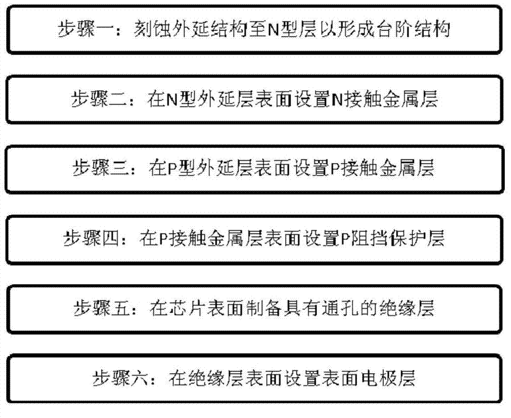
[0054] This embodiment is a preparation example of the flip-chip LED chip in embodiment 1, and the brief process of its preparation method can be found in Figure 5 .

[0055] In order to simplify the view, the schematic diagram of the steps involved in coating the photoresist layer and patterning the photoresist layer is not shown in this embodiment, which is common knowledge in the field, even if no explanation is given, those skilled in the art can understand .

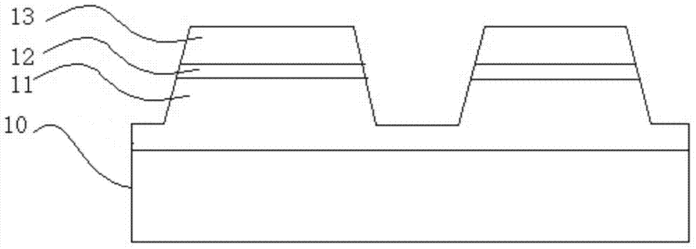
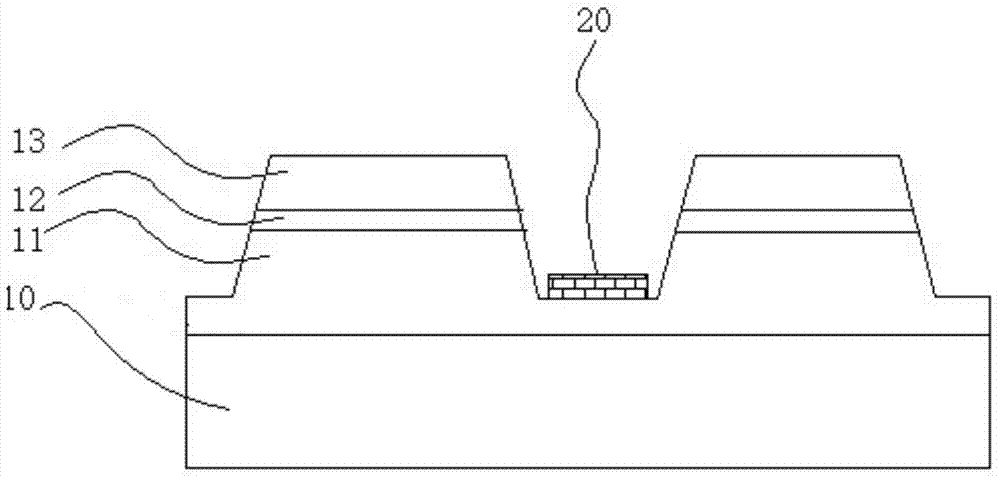
[0056] Embodiment 2 is carried out according to the following steps, for ease of understanding, the following steps are combined Figure 6-9 and image 3 Make an introduction:

[0057] Step 1): Prepare an epitaxial wafer, which includes an epitaxial substrate 100, and an N-type epitaxial layer 101, a light-emitting layer 102, and a P-type epitaxial layer 103 sequentially laminated on the upper surface of the epitaxial substrate; The P-type epitaxial layer 103 upper surface prepares the P contact metal layer 201...

Embodiment 3

[0066] This embodiment is another preparation example of the flip-chip LED chip in embodiment 1, and the brief process of its preparation method can be found in Figure 10 .


PUM


Abstract

The invention provides a flip LED (light-emitting diode) chip with high luminous efficiency and good heat radiating performance and a preparation method thereof. The LED chip comprises an epitaxial substrate, wherein an N type epitaxial layer, a light-emitting layer and a P type epitaxial layer are sequentially laminated on the upper surface of the epitaxial substrate; a concave hole is formed in the P type epitaxial layer, downwards penetrates through the light-emitting layer and extends to the N type epitaxial layer; a P contact metal layer, a P baffle protecting layer and a P surface electrode layer are sequentially laminated on the upper surface of the P type epitaxial layer; the lower surface of the P baffle protecting layer and the upper surface of the P contact metal layer are overlapped; an N contact metal layer and an N surface electrode layer are sequentially laminated on the upper surface of the N type epitaxial layer corresponding to the bottom of the concave hole; a clearance is reserved between the N contact metal layer and the edge of the concave hole; an insulating layer is arranged on the wall surface of the clearance. The flip LED chip provided by the invention has high heat-conducting property and conductivity, and improvement of the luminous efficiency of the LED chip is facilitated by the structure.

Description

technical field [0001] The invention belongs to the field of manufacturing light-emitting devices, and relates to a light-emitting diode chip with a flip-chip structure and a manufacturing method thereof. Background technique [0002] Light-emitting diode (LED) light sources have the advantages of high efficiency, long life, and no harmful substances such as Hg. With the rapid development of LED technology, the brightness and lifespan of LEDs have been greatly improved, making the application of LEDs more and more extensive. From outdoor lighting such as street lights to urban lighting such as decorative lights, they are all used or Replace with LED as light source. [0003] In the semiconductor lighting industry, the structure of LED chips is generally divided into three types: front chip structure, vertical chip structure and flip chip structure. Compared with the other two chip structures, the flip chip structure has the advantages of good heat dissipation performance, ...

Claims


Application Information

Patent Timeline
Patent Type & Authority Applications(China)
IPC IPC(8): H01L33/44H01L33/62H01L33/00
CPCH01L33/005H01L33/44H01L33/62
Inventor 詹东哲肖国伟侯宇曾照明姜志荣万垂铭何贵平
Owner APT ELECTRONICS
Why Eureka
Try Eureka