OLED (Organic Light Emitting Diode) packaging structure and method

A packaging structure and packaging method technology, applied in the direction of organic semiconductor devices, electrical components, electrical solid devices, etc., can solve the problems of not being suitable for large-size panels, affecting display effects, and panel bending, so as to avoid uneven display brightness and increase The effect of bonded area, good sealing and mechanical strength

Active Publication Date: 2015-04-08
TCL CHINA STAR OPTOELECTRONICS TECH CO LTD
View PDF6 Cites 26 Cited by
  • Summary
  • Abstract
  • Description
  • Claims
  • Application Information

AI Technical Summary

Problems solved by technology

However, the glass powder laser sealing technology is not suitable for large-sized panels due to the gaps in the panel. As the panel size increases, the panel is prone to bending, affecting the display effect, and easily broken.

Method used


Image

  • OLED (Organic Light Emitting Diode) packaging structure and method
  • OLED (Organic Light Emitting Diode) packaging structure and method
  • OLED (Organic Light Emitting Diode) packaging structure and method

Examples


Embodiment Construction

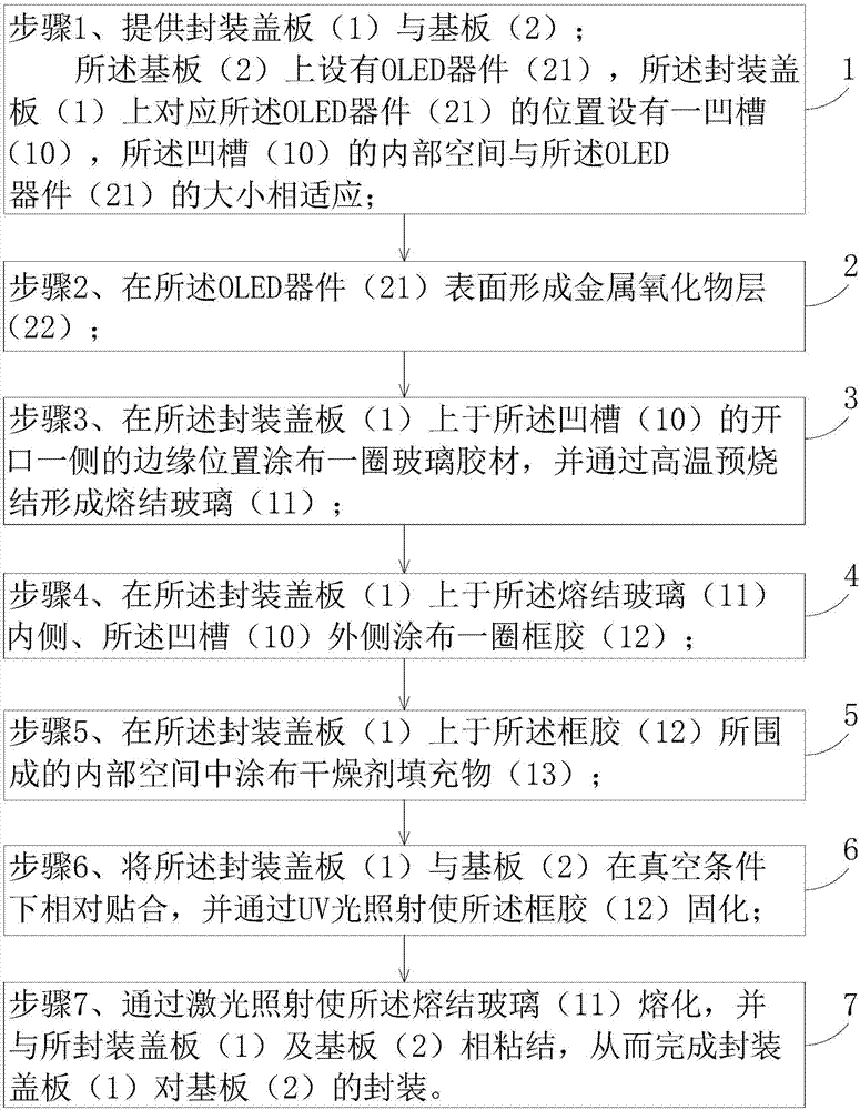
[0036] In order to further illustrate the technical means adopted by the present invention and its effects, the following describes in detail in conjunction with preferred embodiments of the present invention and accompanying drawings.

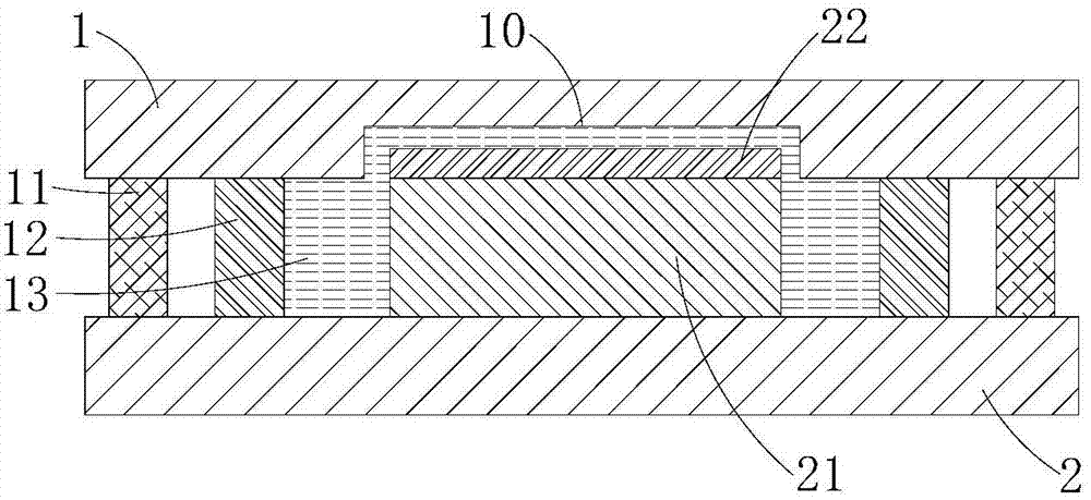
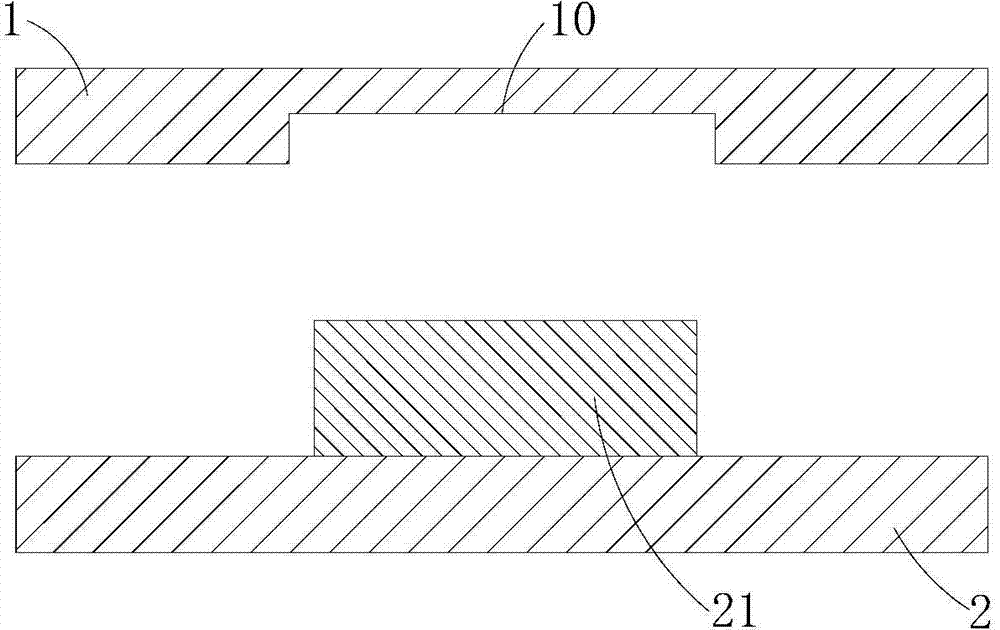
[0037] Such as figure 1 As shown, the present invention provides an OLED packaging structure, including a packaging cover plate 1, a substrate 2 disposed opposite to the packaging cover plate 1, located between the packaging cover plate 1 and the substrate 2 and arranged on the substrate 2 The OLED device 21 on the surface, the metal oxide layer 22 formed on the surface of the OLED device 21, the sealant 12 provided on the periphery of the OLED device 21 to bond the package cover 1 and the substrate 2, and fill the package cover The inner space surrounded by the sealant 12 between the plate 1 and the substrate 2 covers the desiccant filler 13 of the OLED device 21, and is arranged on the periphery of the sealant 12 to bond the packaging cover ...


PUM


Abstract

The invention provides an OLED (Organic Light Emitting Diode) packaging structure and an OLED packaging method. The OLED packaging structure comprises a packaging cover plate, a base plate, an OLED device, a metal oxide layer, frame glue, drying agent fillers and sintered glass, wherein the base plate is opposite to the packaging cover plate; the OLED device is positioned between the packaging cover plate and the base plate and is arranged on the base plate; the metal oxide layer is formed on the surface of the OLED device; the frame glue is arranged at the periphery of the OLED device and is used for gluing the packaging cover plate and the base plate; the drying agent fillers are filled in an internal space, which is positioned between the packaging cover plate and the base plate and is enclosed by the frame glue, and cover the OLED device; the sintered glass is arranged at the periphery of the frame glue and is used for gluing the packaging cover plate and the base plate. According to the structure, the frame glue and the sintered glass are used for packaging; meanwhile, the interior of the frame glue is filled with the drying agent fillers, so that the packaging structure has excellent sealing property and high mechanical strength; moreover, the metal oxide layer is formed on the surface of the internal OLED device, so that the problems of non-uniform brightness of a display and the like caused by the fact that light emitting elements are corroded by the drying agent fillers, particularly liquid-stage drying agents are avoided.

Description

technical field [0001] The invention relates to the field of display technology, in particular to an OLED packaging structure and a packaging method thereof. Background technique [0002] OLED is an Organic Light-Emitting Diode (Organic Light-Emitting Diode), which has the characteristics of self-illumination, high brightness, wide viewing angle, high contrast, flexibility, and low energy consumption. It began to gradually replace traditional liquid crystal displays and was widely used in mobile phone screens, computer monitors, full-color TVs, etc. Unlike traditional liquid crystal display technology, OLED display technology does not require a backlight, and uses very thin coatings of organic materials and glass substrates that emit light when an electric current passes through them. However, because organic materials are easy to react with water vapor or oxygen, as a display device based on organic materials, OLED displays have very high requirements for packaging. [00...

Claims


Application Information

Patent Timeline
Patent Type & Authority Applications(China)
IPC IPC(8): H01L51/52H01L51/56
CPCH10K50/8426H10K50/846H10K50/844H10K71/00H10K2102/00
Inventor 曾维静王宜凡
Owner TCL CHINA STAR OPTOELECTRONICS TECH CO LTD
Why Eureka
Try Eureka