The pcba processing method and pcba board based on the combination of plug-in component technology and patch technology

A technology of PCB board and processing method is applied in the field of circuit board processing to achieve the effect of saving labor costs and material costs, good economic and social benefits, and reducing temperature resistance requirements

Active Publication Date: 2018-10-02
深圳市凯健奥达科技有限公司
View PDF5 Cites 0 Cited by
  • Summary
  • Abstract
  • Description
  • Claims
  • Application Information

AI Technical Summary

Problems solved by technology

[0005] 1. Plug-in process

Method used


Image

  • The pcba processing method and pcba board based on the combination of plug-in component technology and patch technology
  • The pcba processing method and pcba board based on the combination of plug-in component technology and patch technology
  • The pcba processing method and pcba board based on the combination of plug-in component technology and patch technology

Examples


Embodiment Construction

[0030] It should be noted that, in the case of no conflict, the embodiments in the present application and the features in the embodiments can be combined with each other.

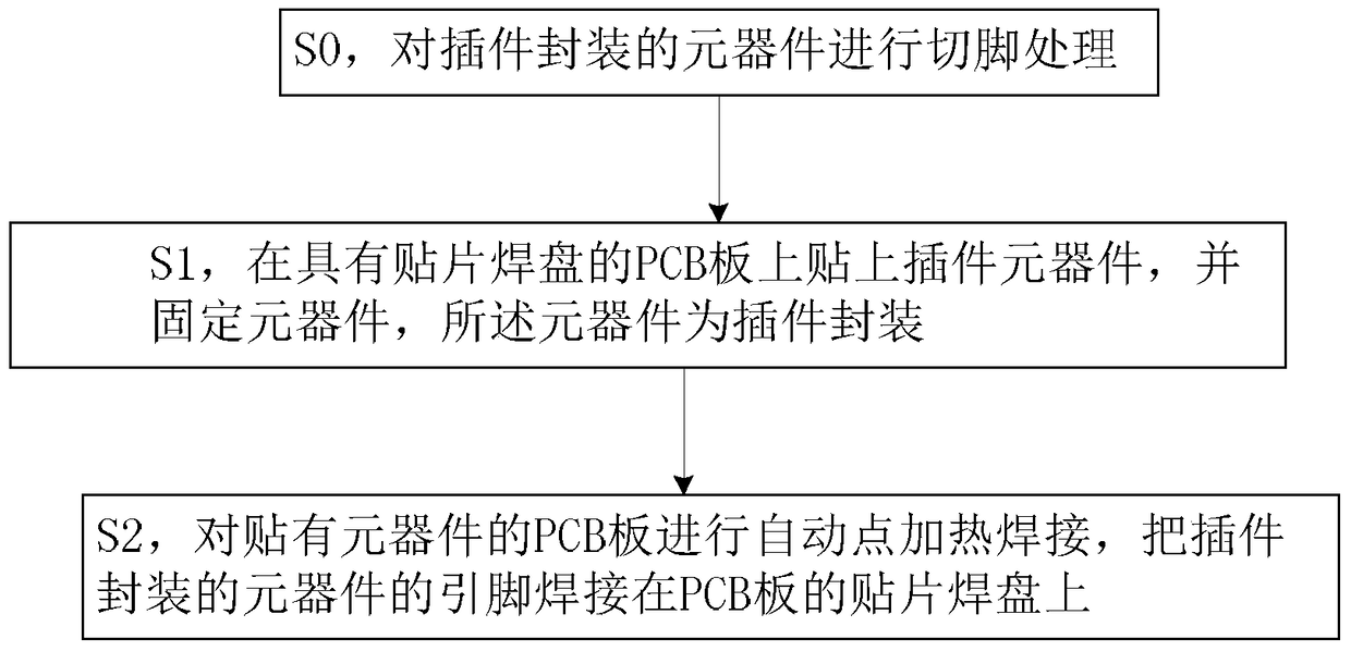
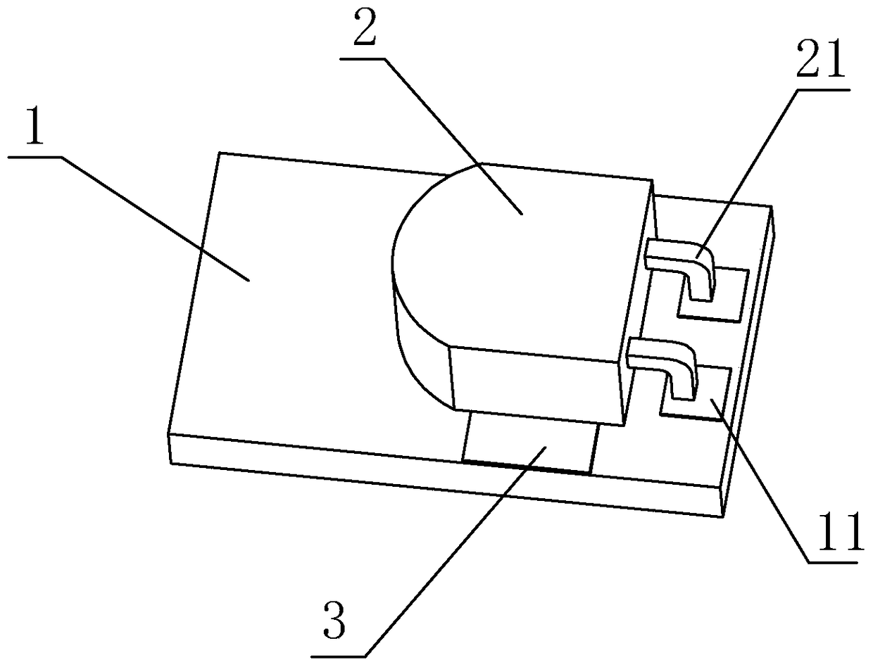
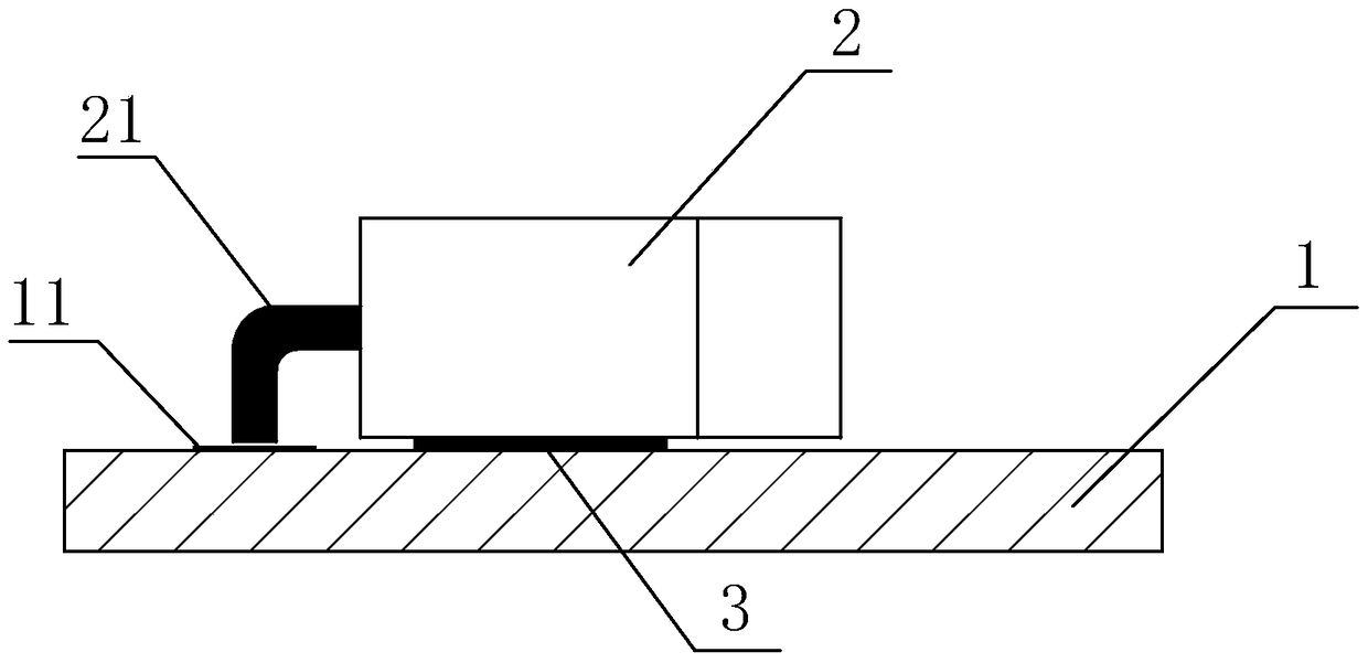
[0031] Such as figure 1 As shown, a PCBA processing method based on the combination of plug-in component technology and patch technology is characterized in that it includes the step: S1, attaching plug-in components on a PCB with patch pads, and fixing the components, The components are plug-in packages; S2, performing automatic spot heating and welding on the PCB with the components attached, and welding the pins of the components in the plug-in package to the patch pads of the PCB. The automatic heating soldering is a non-reflow soldering process, such as using an automatic positioning soldering machine to separately heat and solder the pins of the components in the plug-in package.

[0032] Such as Figure 2 to Figure 4 As shown, the step S1 specifically includes sub-steps: S11, first paste the adhes...


PUM


Abstract

The invention discloses a plug-in component technology and surface mount technology combination based PCBA (printed circuit board assembly) machining method and a PCBA. The method includes the steps: S1, attaching a plug-in component on a PCB with a surface mount bonding pad, and fixing the component which is packaged in a plug-in manner; S2, subjecting the PCB mounted with the component to automatic spot heating welding, and welding pins of the component in plug-in package on the surface mount bonding pad of the PCB. The PCB is provided with the plug-in packaged component and the surface mount bonding pad, and the pins of the plug-in packaged component are welded on the surface mount bonding pad. The advantages of plug-in technology and the surface mount technology are fused, the plug-in packaged component and the PCB with the surface mount ponding pad are utilized, and the automatic spot heating welding technology is combined, so that labor cost and material cost of PCBA machining are saved, the requirement on temperature resistance of the component is lowered, production efficiency and product percent of pass of the PCB are increased, and good social and economic benefits are gained. The method can be widely applied to various PCBA machining technologies.

Description

technical field [0001] The invention relates to the field of circuit board processing, in particular to a PCBA semi-finished product processing method, and the invention also relates to a PCBA board. Background technique [0002] Printed circuit boards, also known as printed circuit boards and printed circuit boards, often use the English abbreviation PCB (Printed circuit board) or write PWB (Printed wire board). The insulating board is used as the base material and cut to a certain size. A conductive pattern with holes (such as component holes, fastening holes, metallized holes, etc.), used to replace the chassis of electronic components installed in the past, and to realize the interconnection between electronic components. Since such boards are made using electronic printing, they are called "printed" circuit boards. [0003] PCBA is the abbreviation of Printed Circuit Board + Assembly in English, that is to say, the empty PCB board passes through the SMT upper part, and...

Claims


Application Information

Patent Timeline
Patent Type & Authority Patents(China)
IPC IPC(8): H05K3/34
CPCH05K1/181H05K3/341H05K2201/10121H05K2203/04
Inventor 李荣尧秦波
Owner 深圳市凯健奥达科技有限公司
Why Eureka
Try Eureka