LDMOS (lateral double-diffused metal oxide semiconductor) transistor structure and formation method thereof

A technology of transistor and gate structure, which is applied in the field of LDMOS transistor structure and its formation, can solve the problem of transistor area increase and achieve the effect of improving breakdown voltage

Inactive Publication Date: 2015-04-15
SEMICON MFG INT (SHANGHAI) CORP
View PDF3 Cites 11 Cited by
  • Summary
  • Abstract
  • Description
  • Claims
  • Application Information

AI Technical Summary

Problems solved by technology

[0012] However, while increasing the size of the shallow trench isolation structure along the direction of the surface of the P-type substrate 01, the area occupied by the transistor is also increased.

Method used


Image

  • LDMOS (lateral double-diffused metal oxide semiconductor) transistor structure and formation method thereof
  • LDMOS (lateral double-diffused metal oxide semiconductor) transistor structure and formation method thereof
  • LDMOS (lateral double-diffused metal oxide semiconductor) transistor structure and formation method thereof

Examples


Embodiment Construction

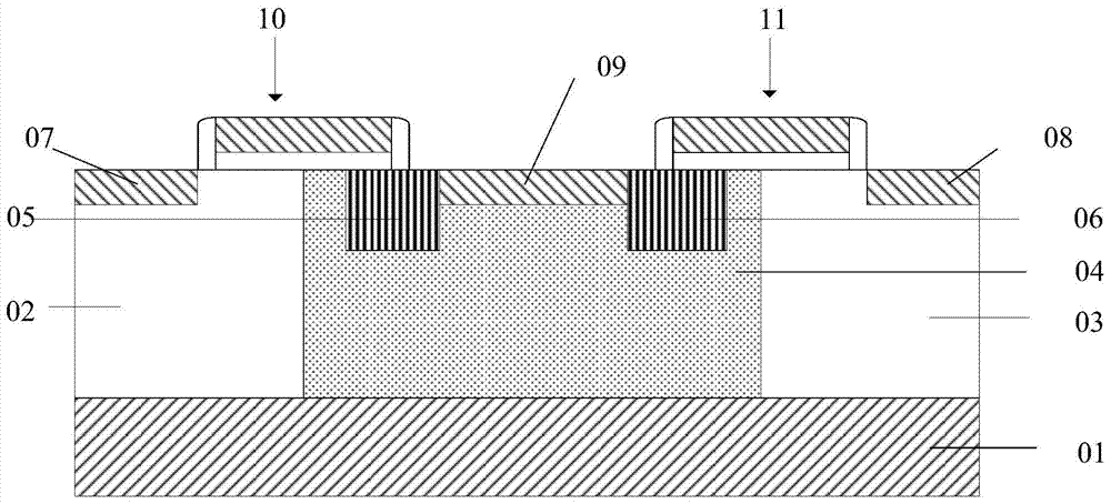
[0070] In the LDMOS transistor structure in the prior art, the size of the STI structure in the horizontal direction is usually increased in the LDMOS transistor, so that the STI structure can share more voltage, thereby increasing the breakdown voltage of the LDMOS transistor. However, while increasing the size of the shallow trench isolation structure in the horizontal direction, the area occupied by the transistor also increases correspondingly.

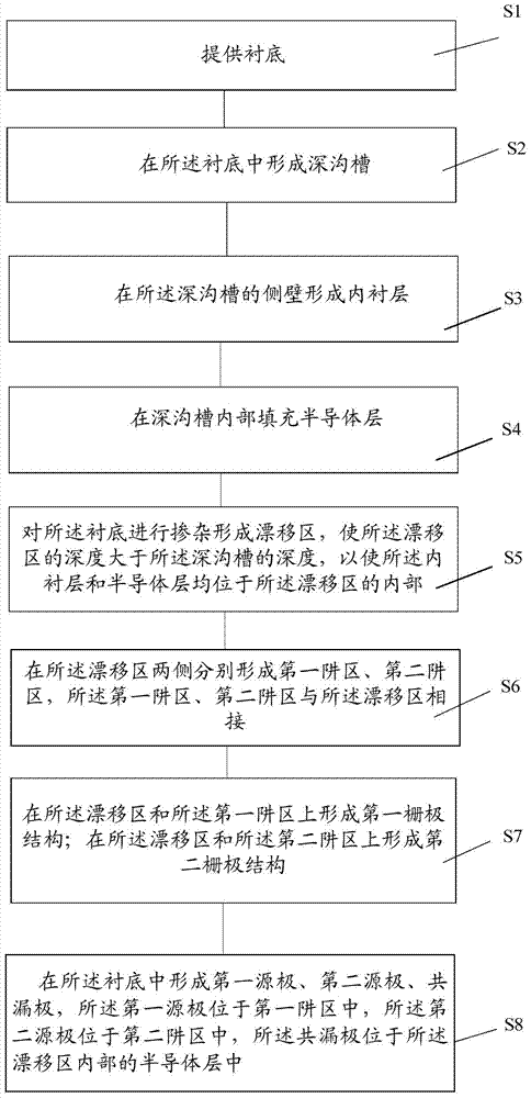
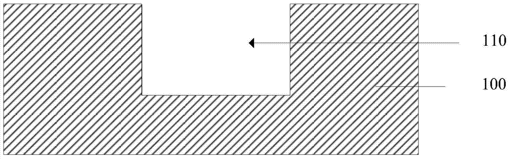
[0071] In order to solve the technical problem, the present invention provides an LDMOS transistor structure and a forming method thereof. The LDMOS transistor structure includes two LDMOS transistors sharing a common drain, the LDMOS transistor structure includes a deep trench, the sidewall of the deep trench is also provided with an inner lining layer, and the common drain is arranged to fill in the In the semiconductor layer of the deep trench, the first source and the second source of the two LDMOS transistors are respectively...


PUM


Abstract

Disclosed are an LDMOS (lateral double-diffused metal oxide semiconductor) transistor structure and a formation method thereof. The formation method includes forming a deep groove in a substrate, forming a liner layer on the side wall of the deep groove, and filling a semiconductor layer in the deep groove; doping the substrate to form a drift area, and enabling the liner layer and the semiconductor layer within the drift area; forming a first trap and a second trap respectively in the substrate on two sides of the drift area, connecting the first trap and the second trap with the drift area; forming a first grid structure on the drift area and the first trap; forming a second grid structure on the drift area and the second trap; forming a common drain in the semiconductor layer exposed by the first grid structure and the second grid structure; forming a first source in the first trap exposed by the first grid structure, and forming a second source in the second trap exposed by the second grid structure. By the LDMOS transistor structure, breakdown voltage of the LDMOS transistor can be increased without increasing the area of the transistor.

Description

technical field [0001] The invention relates to the field of semiconductors, in particular to an LDMOS transistor structure and a forming method thereof. Background technique [0002] Compared with common field effect transistors, LDMOS (lateral double-diffused MOSFET) transistors have obvious advantages in terms of device characteristics such as gain, linearity, switching performance, heat dissipation performance, and reduced number of stages, so they are widely used. [0003] refer to figure 1 , shows a common LDMOS (Lateral Double Diffused Metal Oxide Semiconductor) transistor structure in the prior art. Here, a case where two adjacent N-type transistors share a common drain is used for illustration. LDMOS transistor structures include: [0004] P-type substrate 01; [0005] a first well region 02 disposed in the P-type substrate 01; [0006] a second well region 03 disposed in the P-type substrate 01; [0007] The N-type drift region 04 is disposed between the firs...

Claims


Application Information

Patent Timeline
Patent Type & Authority Applications(China)
IPC IPC(8): H01L21/336H01L21/762H01L21/28H01L21/8234H01L29/40H01L29/06H01L29/78H01L27/088
CPCH01L29/66681H01L29/06H01L29/0611H01L29/4232H01L29/7816
Inventor 魏琰宋化龙
Owner SEMICON MFG INT (SHANGHAI) CORP
Why Eureka
Try Eureka