Unlock instant, AI-driven research and patent intelligence for your innovation.
Display device, array substrate, thin film transistor and fabricating method thereof
What is Al technical title?
Al technical title is built by PatSnap Al team. It summarizes the technical point description of the patent document.
A technology of thin film transistor and manufacturing method, which is applied in the field of display devices and can solve problems such as reduction of on-state current
Inactive Publication Date: 2015-04-22
BOE TECH GRP CO LTD
View PDF4 Cites 15 Cited by
Summary
Abstract
Description
Claims
Application Information
AI Technical Summary
This helps you quickly interpret patents by identifying the three key elements:
Problems solved by technology
Method used
Benefits of technology
Problems solved by technology
[0006] The technical problem to be solved by the present invention is to provide a display device, an array substrate, a thin film transistor and a manufacturing method thereof, so as to overcome the strong off-state current of the TFT in the prior art, which causes the decrease of the on-state current due to the LDD structure when the TFT is working. TFT structure
Method used
Image
Click on the blue label to locate the original text in one second.
Reading with bidirectional positioning of images and text.
Examples
Embodiment 1
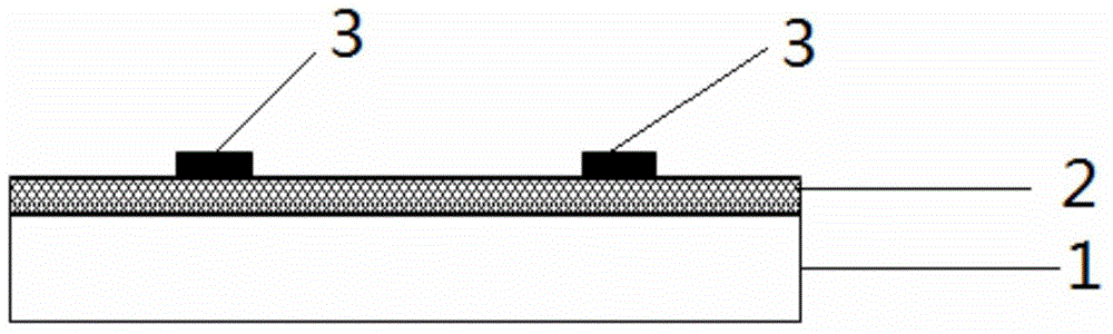
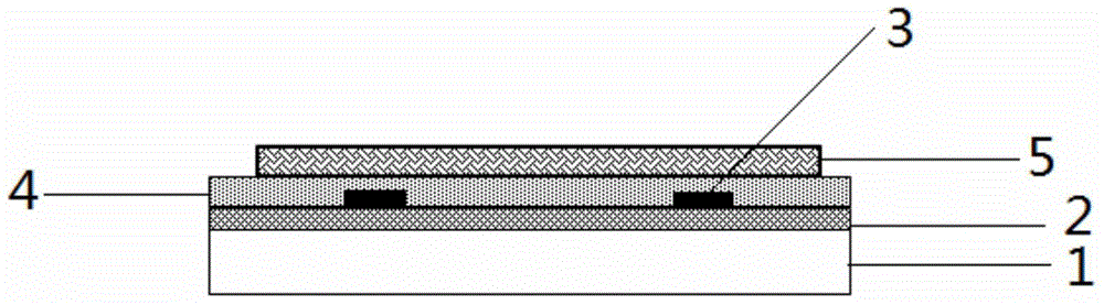
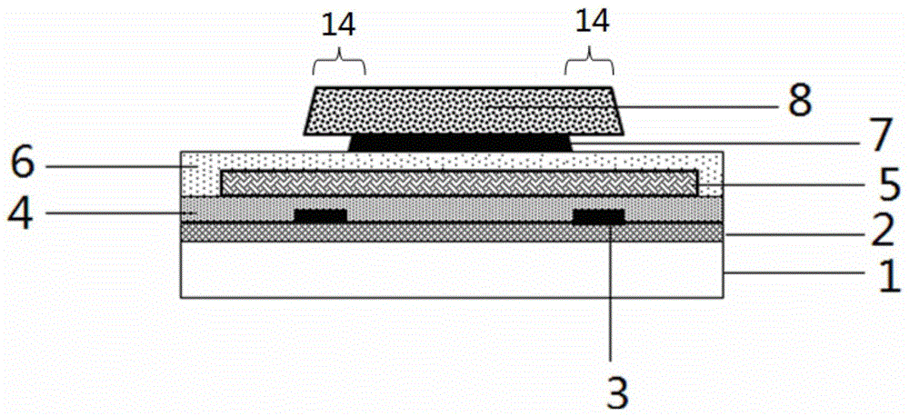
[0041] Such as Figure 6 As shown, the embodiment of the present invention provides an array substrate, including a substrate 1, on which a buffer layer 2, a first gate 3 (ie, a bottom gate) and a first gate insulating layer 4 are provided, and the first An active layer 5 is provided on the gate insulating layer 4, and a second gate insulating layer 6, a second gate 7 (i.e., a top gate), a third gate insulating layer 11, and source-drain electrodes are sequentially provided on the active layer 5. 12 , the source and drain electrodes 12 are on the third gate insulating layer 11 . The outer sides of the region of the active layer 5 corresponding to the second gate 7 are lightly doped source and drain regions 91 and 101 and heavily doped source and drain regions 92 and 102, wherein the lightly doped source region 91 The drain lightly doped region 101 is next to the second gate 7, the source heavily doped region 92 is next to the source lightly doped region 91 and the drain heavi...
Embodiment 2
[0048] Example 2 as Figure 7 As shown, the difference between this embodiment and Embodiment 1 is that there is only a part of the first gate 3 in this embodiment, and it only needs to be disposed under the lightly doped drain region 101 in the region corresponding to the drain electrode.
[0049]The first gate 3 and the second gate 7 also use the advantage of LDD to reduce the off-state current, combined with the working principle of the bottom gate structure, when the TFT is working, that is, when the top gate is applied with gate voltage, the bottom gate is also simultaneously Turn on, so that the LDD region also induces carriers, so that the LDD region can avoid the decrease of the on-state current Ion due to the light doping under the action of the bottom gate electric field and the carriers generated by light doping. Similarly, when the top gate electric field of the TFT is removed, it is in the off state, and the bottom gate also removes its electric field at this time...
Embodiment 3
[0052] Such as Figure 8 As shown, the embodiment of the present invention also provides a manufacturing method based on the array substrate in Embodiment 1, and the specific steps include:
[0053] Step S31, forming the pattern of the first gate on the substrate;
[0054] Step S32, forming a first gate insulating layer on the substrate after the above steps;
[0055] Step S33, forming an active layer on the substrate after the above steps,
[0056] Step S34, forming a second gate insulating layer on the substrate after the above steps;
[0057] Step S35, forming a second gate pattern on the substrate after the above steps;
[0058] Step S36, performing heavy source-drain doping and light source-drain doping on the outside of the region of the active layer corresponding to the second gate; the source lightly doped region and the drain lightly doped region are adjacent to the second gate In the corresponding active layer, the source heavily doped region is adjacent to the s...
PUM
Abstract
The invention relates to the technical field of display processes, and particularly relates to a display device, an array substrate, a thin film transistor (TFT) and a fabricating method thereof. The thin film transistor sequentially comprises a first gate electrode, a first gate insulation layer, an active layer, a second gate insulation layer, a second gate electrode, a third gate insulation layer, a source electrode and a drain electrode, wherein source and drain light-doped regions and source and drain heavy-doped regions are respectively arranged outside regions corresponding to the active layer and the second gate electrode, the source electrode and the drain electrode are electrically connected with the source heavy-doped region and the drain heavy-doped region; the first gate electrode is arranged below the drain light-doped region of the region corresponding to the drain electrode or the first gate electrode is divided into two parts which are respectively arranged below the light-doped regions of the regions corresponding to the source electrode and the drain electrode. The invention provides the display device, the array substrate, the thin film transistor and a fabricating method thereof. The OFF leakage current of the TFT is reduced by virtue of an LDD structure; meanwhile, the effect of the ON current of the TFT is improved by virtue of a bottom gate structure, and the yield of a product is increased.
Description
technical field [0001] The invention relates to the technical field of display technology, in particular to a display device, an array substrate, a thin film transistor and a manufacturing method thereof. Background technique [0002] In LCD (Liquid Crystal Display) or OLED (Organic Light Emitting Diode) displays, each pixel is driven by a TFT (Thin Film Transistor, Thin Film Field EffectTransistor) integrated behind the pixel, so that high-speed, High-brightness, high-contrast display screen information. In the current production technology, polysilicon or amorphous silicon is mostly used to manufacture TFTs. The carrier mobility of polysilicon is 10-200cm2 / V, which is significantly higher than that of amorphous silicon (1cm2 / V), so polysilicon has higher capacitance and storage than amorphous silicon. [0003] For LCDs and OLEDs, TFTs are generally formed on glass substrates. Due to the thermodynamic limitations of glass, the crystallization characteristics of polysilic...
Claims
Application Information
Patent Timeline
Application Date:The date an application was filed.
Publication Date:The date a patent or application was officially published.
First Publication Date:The earliest publication date of a patent with the same application number.
Issue Date:Publication date of the patent grant document.
PCT Entry Date:The Entry date of PCT National Phase.
Estimated Expiry Date:The statutory expiry date of a patent right according to the Patent Law, and it is the longest term of protection that the patent right can achieve without the termination of the patent right due to other reasons(Term extension factor has been taken into account ).
Invalid Date:Actual expiry date is based on effective date or publication date of legal transaction data of invalid patent.

