LED substrate structure and manufacturing method thereof

A technology of a substrate structure and a manufacturing method, which is applied to electrical components, circuits, semiconductor devices, etc., can solve the problems of low light output efficiency of flip-chip LED chips, and achieve the effects of improving axial luminous brightness, improving luminous brightness, and simple process.

Active Publication Date: 2015-04-22
HANGZHOU SILAN MICROELECTRONICS +1
View PDF7 Cites 0 Cited by
  • Summary
  • Abstract
  • Description
  • Claims
  • Application Information

AI Technical Summary

Problems solved by technology

[0007] The purpose of the present invention is to provide an LED substrate structure and its manufacturing method to solve the problem of low light extraction efficiency of existing flip-chip LED chips

Method used


Image

  • LED substrate structure and manufacturing method thereof
  • LED substrate structure and manufacturing method thereof
  • LED substrate structure and manufacturing method thereof

Examples


Embodiment 1

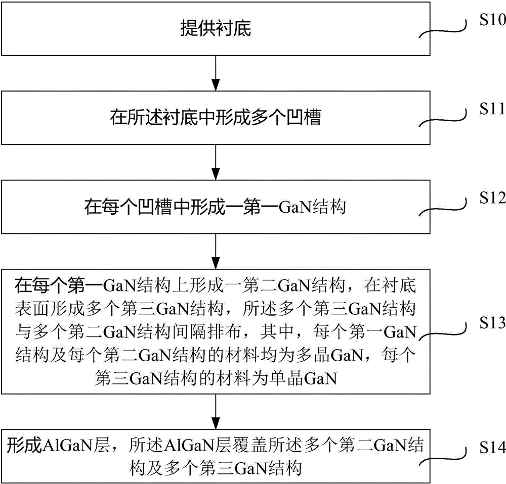
[0055] Please refer to Figure 2 to Figure 9 , which is a schematic diagram of a device structure formed in the method for manufacturing an LED substrate structure according to Embodiment 1 of the present invention.

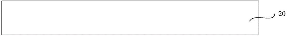
[0056] Such as figure 2 As shown, a substrate 20 is provided, preferably, the substrate 20 is a sapphire substrate.

[0057] Next, a plurality of grooves are formed in the substrate 20, specifically, please refer to Figure 3 ~ Figure 5 .

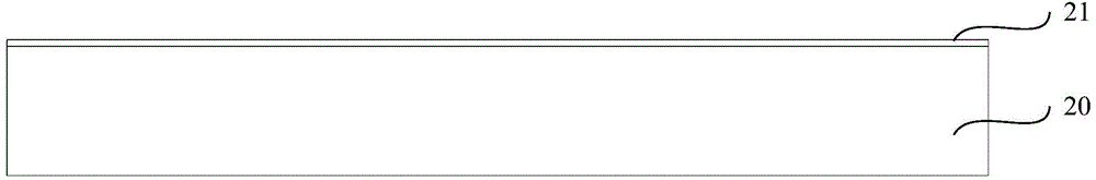
[0058] First, if image 3 As shown, a mask layer 21 is formed on the substrate 20 . Preferably, the material of the mask layer 21 is at least one of silicon dioxide, silicon nitride and silicon oxynitride. In the embodiment of the present application, the mask layer 21 may be formed by an evaporation process, a sputtering process, a PECVD process, or an LPCVD process.

[0059] Next, if Figure 4 As shown, a plurality of openings 22 are formed in the mask layer 21 to expose part of the substrate 20 . Here, a part of th...

Embodiment 2

[0072] The difference between the second embodiment and the first embodiment is that the shape of the groove is triangular, that is, the shape of the first GaN structure is triangular. Specifically, please refer to Figure 10 ~ Figure 17 , which is a schematic diagram of the device structure formed in the method for manufacturing the LED substrate structure according to the second embodiment of the present invention.

[0073] Such as Figure 10 As shown, a substrate 30 is provided, preferably, the substrate 30 is a sapphire substrate.

[0074] Next, a plurality of grooves are formed in the substrate 30, specifically, please refer to Figure 11 ~ Figure 13 .

[0075] First, if Figure 11 As shown, a mask layer 31 is formed on the substrate 30 . Preferably, the material of the mask layer 31 is at least one of silicon dioxide, silicon nitride and silicon oxynitride. In the embodiment of the present application, the mask layer 31 may be formed by an evaporation process, a sp...


PUM


Abstract

The invention provides an LED substrate structure and a manufacturing method of the LED substrate structure. In the LED substrate structure, a first GaN structure and a second GaN structure can enhance transmission of light, further the luminous efficiency of a flip LED chip is improved, and the luminance of the flip LED chip is improved accordingly; a third GaN structure has a condensation function, and consequently the axial luminance of the flip LED chip is improved; in addition, an AlGaN layer can inhibit defects in the second GaN structure and the third GaN structure from extending outwards, defects in the subsequent structures are reduced, and furthermore, the AlGaN layer can improve the breakdown resisting capacity of the flip LED chip and facilitates the improvement on the performance and reliability of the flip LED chip. The manufacturing method of the LED substrate structure is simple in process, high in operability and suitable for large-scale commercialized production, and accords with the future development road of the flip LED chips.

Description

technical field [0001] The invention relates to the technical field of semiconductor optoelectronic chip manufacturing, in particular to an LED substrate structure and a manufacturing method thereof. Background technique [0002] With the improvement of people's living standards, the enhancement of environmental awareness, the continuous improvement of the pursuit of home environment, leisure and comfort. Lamps and lighting are gradually shifting from simple lighting functions to the coexistence of decoration and lighting. It is inevitable that solid-state cold light source LEDs with dual advantages of lighting and decoration will replace traditional light sources and enter people's daily life. [0003] Since the commercialization of GaN-based LEDs in the early 1990s, after more than 20 years of development, its structure has become mature and perfect, and it has been able to meet people's current needs for lighting decoration; but it must completely replace traditional ligh...

Claims


Application Information

Patent Timeline
IPC IPC(8): H01L33/10H01L33/22H01L33/00
CPCH01L33/0075H01L33/025H01L33/48H01L33/58H01L2933/0033
Inventor 张昊翔丁海生李东昇江忠永
Owner HANGZHOU SILAN MICROELECTRONICS
Why Eureka
Try Eureka