Grating subdivision device and method based on FPGA

A technology of grating and differential amplifying circuit, which is applied in the direction of using optical devices to transmit sensing components, etc., can solve the problems that the subdivision device cannot meet the requirements, the speed is not fast enough, and the subdivision multiple is high.

Inactive Publication Date: 2015-04-29
KUNMING UNIV OF SCI & TECH
View PDF7 Cites 10 Cited by
  • Summary
  • Abstract
  • Description
  • Claims
  • Application Information

AI Technical Summary

Problems solved by technology

Quadruple frequency resolution subdivision and resistance chain phase shift subdivision circuit is simple but the subdivision multiple is very low
Phase-locked frequency multiplication subdivision and carrier modulation subdivision have high requirements on the frequency of the encoder input signal. If the frequency changes too fast, the subdivision error will be large
The amplitude segmentation method has a high subdivision multiple and is suitable for high-multiplier subdivision occasions. However, the method of combining signal conditioning circuits with single-chip microcomputers or DSPs is usually used. Because the processing speed of single-chip microcomputers and DSPs is not fast enough when processing subdivision algorithms, the subdivision device is in the High-precision and high-resolution subdivision occasions cannot meet the requirements, and can only achieve hundreds of subdivisions at most

Method used


Image

  • Grating subdivision device and method based on FPGA
  • Grating subdivision device and method based on FPGA
  • Grating subdivision device and method based on FPGA

Examples


Embodiment 1

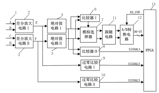
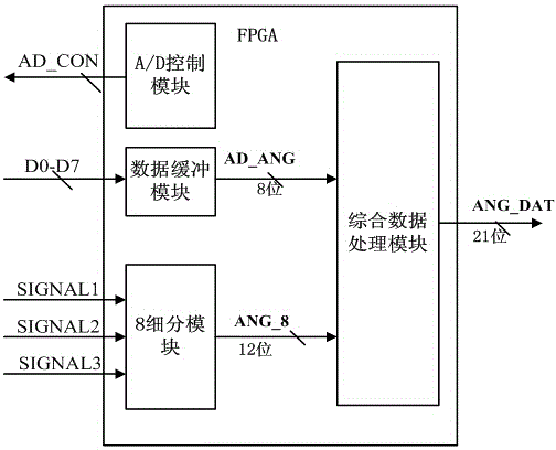
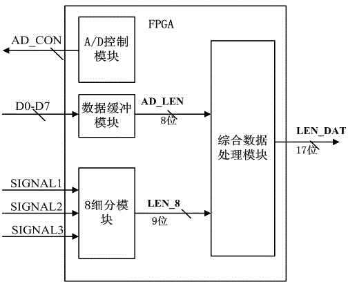
[0049] Embodiment 1: as Figure 1-7 As shown, a raster subdivision device based on FPGA includes input signal 1, differential amplifier circuit I2, differential amplifier circuit II3, absolute value circuit I4, absolute value circuit II5, comparator I6, analog selector 7, comparator II8 , Zero-crossing comparison circuit I9, zero-crossing comparison circuit II10, follower circuit 11, A / D conversion circuit 12, FPGA device 13;

[0050] Wherein, the FPGA device 13 outputs a signal to control the clock and the chip selection terminal of the A / D conversion circuit 12;

[0051] After the input signal 1 passes through the differential amplifier circuit I2 and the differential amplifier circuit II3: the zero-crossing comparison circuit I9 and the zero-crossing comparison circuit II10 generate a 2-bit level signal; at the same time, the absolute value signal is obtained through the absolute value circuit I4 and the absolute value circuit II5: The absolute value signal passes through ...

Embodiment 2

[0067] Embodiment 2: as Figure 1-7 As shown, a raster subdivision device based on FPGA includes input signal 1, differential amplifier circuit I2, differential amplifier circuit II3, absolute value circuit I4, absolute value circuit II5, comparator I6, analog selector 7, comparator II8 , Zero-crossing comparison circuit I9, zero-crossing comparison circuit II10, follower circuit 11, A / D conversion circuit 12, FPGA device 13;

[0068] Wherein, the FPGA device 13 outputs a signal to control the clock and the chip selection terminal of the A / D conversion circuit 12;

[0069] After the input signal 1 passes through the differential amplifier circuit I2 and the differential amplifier circuit II3: the zero-crossing comparison circuit I9 and the zero-crossing comparison circuit II10 generate a 2-bit level signal; at the same time, the absolute value signal is obtained through the absolute value circuit I4 and the absolute value circuit II5: The absolute value signal passes through ...

Embodiment 3

[0076] Embodiment 3: as Figure 1-7 As shown, a raster subdivision device based on FPGA includes input signal 1, differential amplifier circuit I2, differential amplifier circuit II3, absolute value circuit I4, absolute value circuit II5, comparator I6, analog selector 7, comparator II8 , Zero-crossing comparison circuit I9, zero-crossing comparison circuit II10, follower circuit 11, A / D conversion circuit 12, FPGA device 13;

[0077] Wherein, the FPGA device 13 outputs a signal to control the clock and the chip selection terminal of the A / D conversion circuit 12;

[0078] After the input signal 1 passes through the differential amplifier circuit I2 and the differential amplifier circuit II3: the zero-crossing comparison circuit I9 and the zero-crossing comparison circuit II10 generate a 2-bit level signal; at the same time, the absolute value signal is obtained through the absolute value circuit I4 and the absolute value circuit II5: The absolute value signal passes through ...


PUM


Abstract

The invention relates to a grating subdivision device and a grating subdivision method based on an FPGA (field programmable gate array), and belongs to the technical field of grating subdivision processing. An output signal of an FPGA device controls the clock and the chip selection terminal of an A / D conversion circuit; after an input signal passes through a differential amplification circuit I and a differential amplification circuit II: a two-position level signal is generated by a zero-crossing comparison circuit I and a zero-crossing comparison circuit II; besides, an absolute value signal is obtained by an absolute value circuit I and an absolute value circuit II: a one-position level signal is obtained from the absolute value signal through a comparator II, and each cycle of a sine signal output by a reading head is divided into 8 linear regions from the absolute value signal through a comparator I, an analog selector, a following circuit and the A / D conversion circuit, and the 8 regions are subdivided one by one to obtain an 8-position level signal. According to the device and the method, the calculating speed of a subdivided data processing algorithm is increased, the defect of low calculating speed caused by a singlechip microcomputer and an DSP (digital signal processor) is overcome, and the subdivision multiple is improved.

Description

technical field [0001] The invention relates to an FPGA-based raster subdivision device and method, and belongs to the technical field of raster subdivision processing. Background technique [0002] As a tool for precision measurement, gratings have been widely used in precision instruments, large-stroke precision positioning, and high-precision machining. The grating measurement technique is based on the moiré fringes formed by the grating. Due to the relative movement of two stacked gratings, there will be periodic changes in light intensity. This optical signal is converted into a periodic electrical signal by photoelectricity. After a series of processing on this electrical signal, the relative movement of the grating can be obtained. the amount of displacement. [0003] By further subdividing the moiré fringes, the grating measurement can obtain higher precision. Moiré fringe subdivision methods include optical subdivision, mechanical subdivision and electronic subdi...

Claims


Application Information

Patent Timeline
Patent Type & Authority Applications(China)
IPC IPC(8): G01D5/34
Inventor 李彬华丁旭
Owner KUNMING UNIV OF SCI & TECH
Why Eureka
Try Eureka