Method and system for preparing silicon-based III-V gallium arsenide semiconductor material

A gallium arsenide and semiconductor technology, which is applied in semiconductor/solid-state device manufacturing, electrical components, circuits, etc., can solve the problem of inability to manufacture large-scale high-quality silicon-based epitaxial III-V semiconductor materials, and reduce material production cost, lower dislocation density in the upper layer, and reduced strain energy

Active Publication Date: 2015-04-29
BEIJING UNIV OF POSTS & TELECOMM
View PDF3 Cites 9 Cited by
  • Summary
  • Abstract
  • Description
  • Claims
  • Application Information

AI Technical Summary

Problems solved by technology

[0006] The invention provides a silicon-based III-V group gallium arsenide semiconductor material preparation method and system to solve the t

Method used


Image

  • Method and system for preparing silicon-based III-V gallium arsenide semiconductor material
  • Method and system for preparing silicon-based III-V gallium arsenide semiconductor material
  • Method and system for preparing silicon-based III-V gallium arsenide semiconductor material

Examples


preparation example Construction

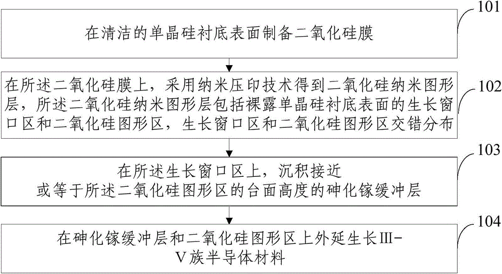
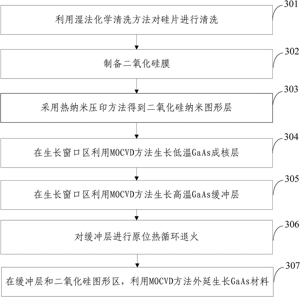
[0064] Embodiments of the present invention firstly provide a method for preparing a silicon-based III-V gallium arsenide semiconductor material, see figure 1 , the method includes:

[0065] Step 101: preparing a silicon dioxide film on the surface of a clean single crystal silicon substrate.

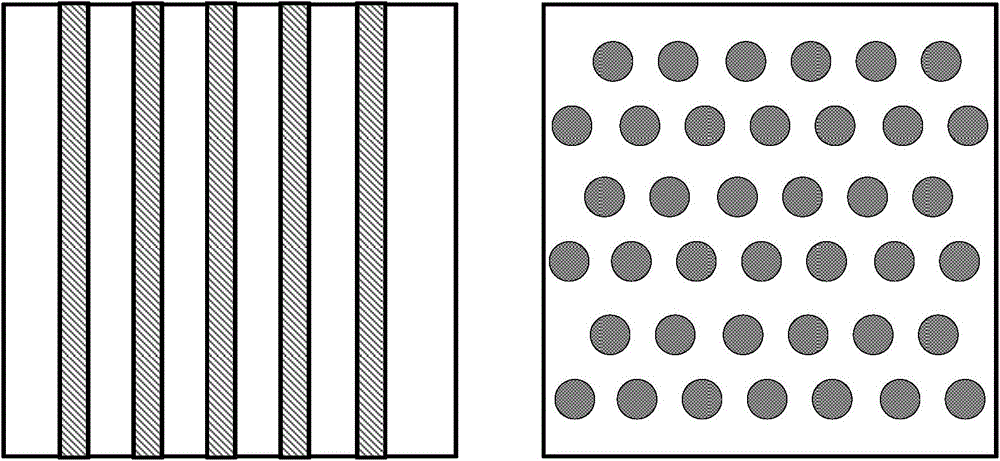
[0066] Step 102: On the silicon dioxide film, use nanoimprint technology to obtain a silicon dioxide nano-patterned layer, the silicon dioxide nano-patterned layer includes a growth window area that exposes the surface of the single crystal silicon substrate, and silicon dioxide The graphic area, the growth window area and the silicon dioxide graphic area are distributed alternately.

[0067] Step 103: On the growth window area, deposit a gallium arsenide buffer layer close to or equal to the mesa height of the silicon dioxide pattern area.

[0068] Step 104: Epitaxially grow III-V group semiconductor material on the gallium arsenide buffer layer and the silicon dioxide pattern region...


PUM

PropertyMeasurementUnit
Thicknessaaaaaaaaaa
Thicknessaaaaaaaaaa
Thicknessaaaaaaaaaa

Abstract

The invention provides a method and a system for preparing a silicon-based III-V gallium arsenide semiconductor material. The method comprises the following steps: preparing a silicon dioxide film on a clean single crystal silicon substrate surface; obtaining a silicon dioxide nanometer pattern layer on the silicon dioxide film by adopting the nanometer imprinting technology, wherein the silicon dioxide nanometer pattern layer comprises a growth window area exposed on the single crystal silicon substrate surface and a silicon dioxide pattern area, and the growth window area and the silicon dioxide pattern area are arranged in a staggered manner; depositing a galium arsenide buffer layer on the growth window area, wherein the height of the galium arsenide buffer layer is close to or equal to that of a table surface of the silicon dioxide pattern area; growing the III-V semiconductor material on the galium arsenide buffer layer and the silicon dioxide pattern area in an extension manner. According to the method, the silicon dioxide nanometer pattern layer is prepared by adopting the nanometer imprinting technology to be used as a pattern substrate for growth of the semiconductor material, and the problem of limitation of material sizes is solved, so that the growth and the preparation of industrial materials are facilitated, the material production cost is effectively lowered, and the method has a broad application prospect.

Description

technical field [0001] The invention relates to the field of semiconductor materials, in particular to a method and system for preparing silicon-based III-V gallium arsenide semiconductor materials. Background technique [0002] The epitaxial growth technology of large lattice mismatch heterostructure materials with no stress and low dislocation density is one of the main development directions of next-generation optoelectronic devices and multifunctional optoelectronic integrated chips. In particular, the high-quality combination of silicon materials developed in microelectronics technology with III-V direct bandgap semiconductor materials such as gallium arsenide has become the best solution for optoelectronic integration technology. However, epitaxially growing III-V semiconductor materials such as device-grade gallium arsenide (GaAs) on silicon substrates has always been a difficult problem in the field of silicon-based material research in the world. [0003] In order ...

Claims


Application Information

Patent Timeline
IPC IPC(8): H01L21/20H01L21/18
CPCH01L21/02381H01L21/02546H01L21/02612
Inventor 王俊李玉斌邓灿王一帆白一鸣王琦段晓峰张霞黄永清
Owner BEIJING UNIV OF POSTS & TELECOMM
Why Eureka
Try Eureka