Manufacturing method of semiconductor device

A semiconductor and device technology, which is applied in the field of semiconductor device preparation, can solve the problems of poor wafer yield and affect the electrical performance of the device, and achieve the effect of improving electrical performance, eliminating aluminum residue, and avoiding the formation of aluminum oxide

Active Publication Date: 2017-11-24
SEMICON MFG INT (SHANGHAI) CORP
View PDF5 Cites 0 Cited by
  • Summary
  • Abstract
  • Description
  • Claims
  • Application Information

AI Technical Summary

Problems solved by technology

Figure 5 It is a scanning electron picture of the aluminum residue 123. Due to the existence of the aluminum residue 123, the yield rate of the entire wafer is poor, thereby affecting the electrical performance of the device

Method used


Image

  • Manufacturing method of semiconductor device
  • Manufacturing method of semiconductor device
  • Manufacturing method of semiconductor device

Examples


preparation example Construction

[0032] The core idea of ​​the present invention is to provide a method for preparing a semiconductor device, including:

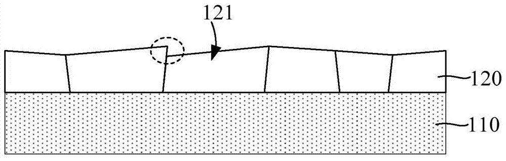
[0033] Step S11, providing a semiconductor substrate;

[0034] Step S12, preparing a metal layer on the semiconductor substrate;

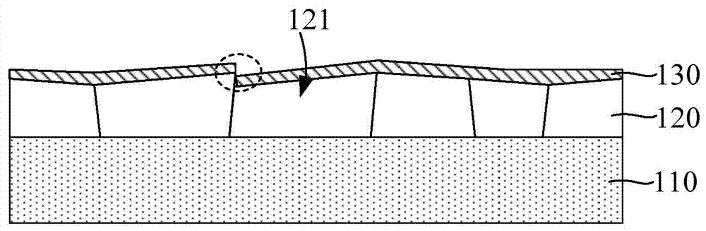
[0035] Step S13, preparing an oxidation barrier layer on the metal layer;

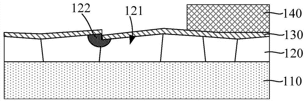
[0036] Step S14, performing an oxidation process so that a metal oxide layer is formed on the surface of the metal layer where the metal layer is in contact with the oxidation barrier layer;

[0037] Step S15, selectively etching the metal layer, the metal oxide layer will block chemical reagents from oxidizing the metal layer, avoiding the formation of local aluminum oxide, thereby reducing or eliminating the formation of aluminum residues, so as to improve the device electrical properties.


PUM


Abstract

The invention discloses a method for preparing a semiconductor device, comprising: providing a semiconductor substrate; preparing a metal layer on the semiconductor substrate; preparing an oxidation barrier layer on the metal layer; performing an oxidation process so that the metal layer A metal oxide layer is formed on the surface of the metal layer in contact with the oxidation barrier layer; and the metal layer is selectively etched. The preparation method of the semiconductor device provided by the present invention first performs an oxidation process, so that a metal oxide layer is formed on the surface of the metal layer where the metal layer is in contact with the oxidation barrier layer, and during selective etching of the metal layer, The metal oxide layer can block chemical reagents from oxidizing the metal layer and avoid the formation of local aluminum oxide, thereby reducing or eliminating the formation of aluminum residues to improve the electrical performance of the device.

Description

technical field [0001] The invention relates to the technical field of semiconductors, in particular to a method for preparing a semiconductor device. Background technique [0002] Metallization is the process of depositing a metal film on an insulating dielectric film during chip manufacturing, and then patterning it to form interconnected metal lines and hole-filling plugs for integrated circuits. Interconnect refers to the wiring made of conductive materials such as aluminum, polysilicon or copper to transmit electrical signals to different parts of the chip. Interconnects are also used as common metal connections between on-chip devices and the overall package . A contact refers to a connection between a device in a silicon chip and the first metal layer on the silicon surface. A via is an opening that passes through various dielectric layers to form an electrical path from a certain metal layer to another adjacent metal layer. [0003] In semiconductor manufacturing,...

Claims


Application Information

Patent Timeline
Patent Type & Authority Patents(China)
IPC IPC(8): H01L21/768H01L21/3213
Inventor 康晓春李志超
Owner SEMICON MFG INT (SHANGHAI) CORP
Why Eureka
Try Eureka