Supercharge Your Innovation With Domain-Expert AI Agents!

Optical switch array module and chamfered optical fiber array packaging method

A technology of optical switch array and optical fiber array, applied in the coupling of optical waveguide, light guide, optics, etc., can solve the problems of high loss, unfavorable high-speed signal transmission, unsuitable for high-integration packaging, etc.

Inactive Publication Date: 2015-05-06
INST OF SEMICONDUCTORS - CHINESE ACAD OF SCI
View PDF3 Cites 3 Cited by
  • Summary
  • Abstract
  • Description
  • Claims
  • Application Information

AI Technical Summary

Problems solved by technology

The optoelectronic integrated package of the traditional optical switch array module generally adopts the wire bond method, which will generate high loss, crosstalk and loss, which are not conducive to the transmission of high-speed signals, and are not suitable for future high-integration packaging requirements.
[0003] With the further development of the Internet and the advent of the Internet of Things and the era of big data, highly integrated and ultra-highly integrated optical switch array devices will become inevitable, and the packaging problems faced by high-density and highly integrated optical switch array modules are also It will follow that the use of FLIP CHIP technology and 3D stacked packaging based on TSV technology can greatly increase the integrated packaging density of the optical switch array and make the parasitic inductance, resistance, capacitance, etc. of the bonded device more than traditional WB technology bonding reduces by an order of magnitude, and at the same time greatly increases the speed of signal exchange. However, in this packaging form, since the optical switch chip is flipped on the carrier board or other chips, the optical coupling structure faces downward. The alignment of the optical coupling structure in the optical switch chip has caused considerable technical difficulty. The practical packaging design of the optical fiber / waveguide coupling device must be comprehensively considered from the aspects of optics, electricity, mechanics, and heat. This patent proposes a The packaging method of the angle-cut optical fiber array can solve this problem very well, and the process is simple and the reliability is high, which can fully adapt to future industrial production

Method used


Image

  • Optical switch array module and chamfered optical fiber array packaging method
  • Optical switch array module and chamfered optical fiber array packaging method

Examples


Embodiment Construction

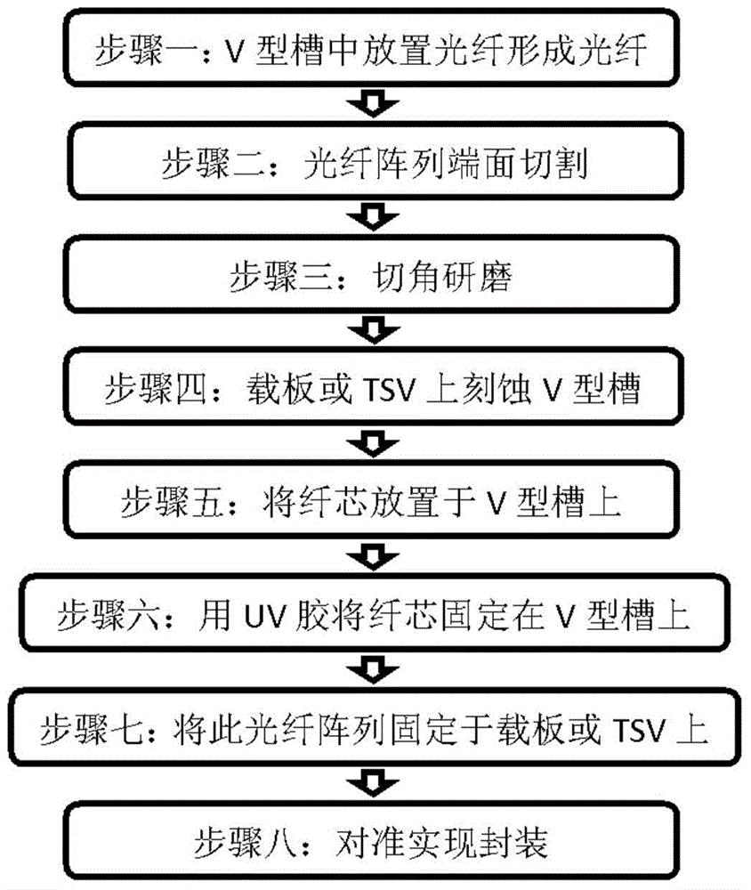
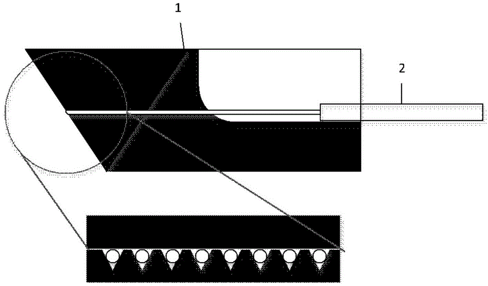
[0018] see figure 1 and figure 2 As shown, the present invention provides a packaging method for an optical switch array module and a cut-angle optical fiber array, including the following steps:

[0019] Step 1: Place the optical fiber 2 in the V-groove fixture 1 to form an optical fiber array, and the angle of the V-groove on the V-groove fixture 1 is 120-30 degrees;

[0020] Step 2: The end face of the optical fiber array formed in the V-groove fixture 1 is cut once to form a consistent cut angle, and the angle of the cut angle formed by the cutting is 45 degrees;

[0021] Step 3: Grinding the chamfer formed by one-time cutting;

[0022] Step 4: Etching a V-shaped groove on a carrier or the TSV on the carrier, the material of the carrier is a polymer-based composite material, and the angle of the V-groove on the carrier or the TSV is 120 degrees -30 degrees;

[0023] Step 5: Fix the fiber core of the optical fiber 2 on the carrier plate or the V-groove etched on the TS...


PUM

PropertyMeasurementUnit
Angleaaaaaaaaaa

Abstract

An optical switch array module and chamfered optical fiber array packaging method comprises the steps of 1 arranging optical fibers in a V-shaped groove clamp to form an optical fiber array, 2 conducting one-time cutting on the end face of the optical fiber array formed in the V-shaped groove clamp to form consistent chamfers, 3 grinding the chamfers formed through one-time cutting, 4 etching a V-shaped groove in a carrier plate or a TSV on the carrier plate, 5 fixing fiber cores of the optical fibers to the V-shaped groove formed in the carrier plate or the TSV on the carrier plate, 6 using an adhesive to fix the fiber cores of the optical fibers and the V-shaped groove formed in the carrier plate or the TSV on the carrier plate, 7 fixing an optical switch array to the carrier plate or the TSV on the carrier plate, 8 achieving coupling between the optical switch array and the optical fiber array on a microscopic alignment platform and performing fixing to complete package. The optical switch array module and chamfered optical fiber array packaging method can ensure that distances among the fiber cores are certain values.

Description

technical field [0001] The invention belongs to the technical field of optoelectronic device packaging, and in particular relates to a packaging method for an optical switch array module and an angle-cut optical fiber array. Background technique [0002] In modern optical communication technology, optical switch is an indispensable device. However, only when optical switch units (such as 1x2, 2x2 switches) are formed into a switch matrix, integrated with corresponding circuits, and packaged into modules, can they be truly applied to optical communication networks. The optoelectronic integrated packaging of the traditional optical switch array module generally adopts the wire bond method, which will cause high loss, crosstalk and loss, which are not conducive to the transmission of high-speed signals, and are not suitable for the future high-integration packaging requirements. [0003] With the further development of the Internet and the advent of the Internet of Things and ...

Claims


Application Information

Patent Timeline
IPC IPC(8): G02B6/24
CPCG02B6/3636G02B6/35
Inventor 张博李显尧李智勇俞育德
Owner INST OF SEMICONDUCTORS - CHINESE ACAD OF SCI
Features
  • R&D
  • Intellectual Property
  • Life Sciences
  • Materials
  • Tech Scout
  • Unparalleled Data Quality
  • Higher Quality Content
  • 60% Fewer Hallucinations
Learn More