Field effect device and preparation method thereof

A field effect and device technology, which is applied in the field of field effect devices and its preparation, can solve the problems of reducing the integration density of transistors, increasing the substrate area, and damaging the epitaxial layer, etc., so as to improve engineering flexibility, strengthen voltage control capabilities, reduce The effect of subthreshold swing

Active Publication Date: 2015-05-13
HUAWEI TECH CO LTD
View PDF4 Cites 23 Cited by
  • Summary
  • Abstract
  • Description
  • Claims
  • Application Information

AI Technical Summary

Problems solved by technology

[0006] 1. The conduction band of the source region overlaps with the valence band of the channel, and the resulting tunneling mechanism is a point tunneling mechanism, that is, the carrier tunneling direction is not in the same direction as the gate electric field, so the electrostatic control effect of the gate voltage is weak, and the load The efficiency of current tunneling is low;
[0007] 2. The electric field in the drain region interferes with the formation of the tunneling junction, affects the threshold voltage of the device, and degrades the subthreshold swing at the same time;
[0008] 3. The traditional TFET structure is a planar structure, which occupies a large substrate area and affects the integration density
[0011] However, the substrate area consumed by the device also increases, thereby reducing the integration density of the transistor. In addition, the planar structure adopts the source replacement technology, which will damage the epitaxial layer, resulting in a decrease in device characteristics.

Method used


Image

  • Field effect device and preparation method thereof
  • Field effect device and preparation method thereof
  • Field effect device and preparation method thereof

Examples


Embodiment Construction

[0059] Embodiments of the present invention provide a field effect device and a manufacturing method thereof, so as to solve the above-mentioned various defects in existing tunneling transistors.

[0060] In order to enable those skilled in the art to better understand the solutions of the present invention, the following will clearly and completely describe the technical solutions in the embodiments of the present invention in conjunction with the drawings in the embodiments of the present invention. Obviously, the described embodiments are only It is an embodiment of a part of the present invention, but not all embodiments. Based on the embodiments of the present invention, all other embodiments obtained by persons of ordinary skill in the art without making creative efforts shall fall within the protection scope of the present invention.

[0061] In the following, specific examples will be used to describe in detail respectively.

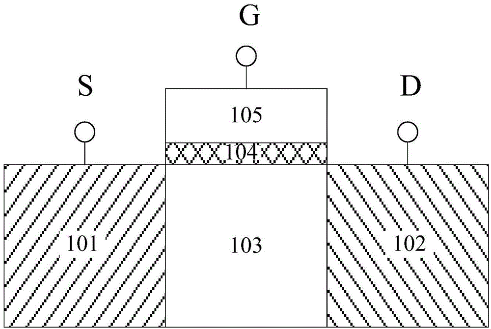
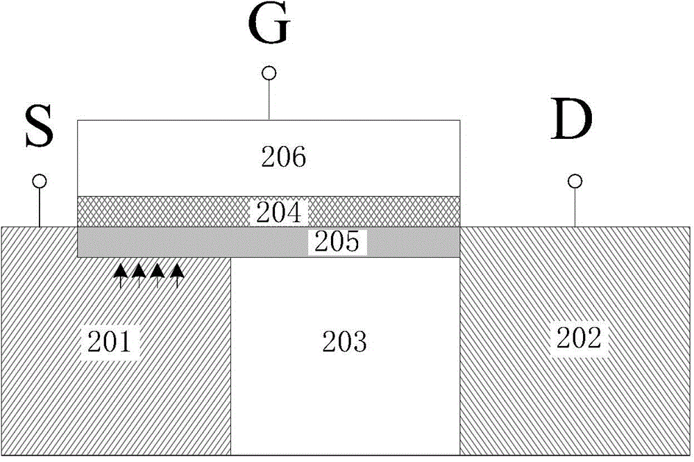
[0062] see figure 2 , an embodiment of ...


PUM


Abstract

The invention discloses a field effect device and a preparation method thereof. The field effect device and the preparation method thereof are used for solving the disadvantages of an existing tunneling transistor. The field effect device comprises a semiconductor substrate with a first doping type, a drain region formed at the surface of the semiconductor substrate and having the first doping type, a convex body formed at the surface of the drain region, a grid formed at the surface of the drain region outside the convex body and higher than the convex body, and gate dielectric layers located between the grid and the drain region and between the grid and the convex body; a semiconductor film formed at the surface of the structure composed of the gate dielectric layers and convex body serves as a pocket layer; a source region is formed at the surface of the pocket layer, and the source region is a semiconductor substrate with a second doping type; the convex body serves as a channel between the drain region and source region.

Description

technical field [0001] The invention relates to the technical field of semiconductors, in particular to a field effect device and a preparation method thereof. Background technique [0002] With the evolution of semiconductor manufacturing technology, the size of electronic devices is gradually reduced, bringing improvements in chip speed, integration, power consumption, and cost. However, as the size of electronic devices approaches the physical limit, the power density of chips also increases. It has become a bottleneck restricting the evolution of semiconductor technology. [0003] In order to continue to improve the chip characteristics of the new process technology, the power consumption of the transistor must be reduced. The most effective way to reduce the power consumption of the transistor is to reduce the supply voltage, but due to the metal oxide semiconductor field effect transistor (Metal Oxide Semiconductor Field Effect) Transistor, MOSFET) is limited by the c...

Claims


Application Information

Patent Timeline
Patent Type & Authority Applications(China)
IPC IPC(8): H01L29/739H01L21/331
Inventor 杨喜超赵静张臣雄
Owner HUAWEI TECH CO LTD
Why Eureka
Try Eureka