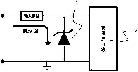
A Transient Voltage Suppressor Structure with Ultra-Deep Trench
A transient voltage suppression, deep trench technology, applied in semiconductor/solid-state device manufacturing, circuits, electrical components, etc., to achieve the effect of device size reduction
- Summary
- Abstract
- Description
- Claims
- Application Information
AI Technical Summary
Problems solved by technology
Method used
Image

Examples
Embodiment Construction
[0030] The following will clearly and completely describe the technical solutions in the embodiments of the present invention. Obviously, the described embodiments are only some of the embodiments of the present invention, rather than all the embodiments. Based on the embodiments of the present invention, all other embodiments obtained by persons of ordinary skill in the art without making creative efforts belong to the protection scope of the present invention.
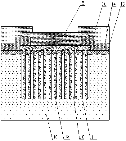
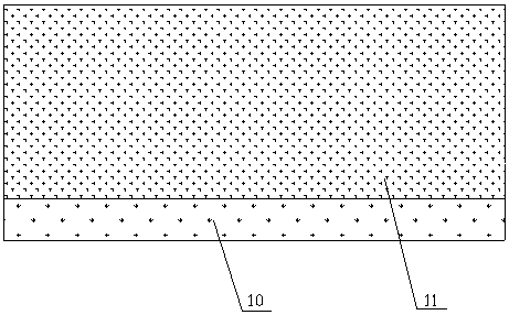
[0031] Such as image 3 As shown, it discloses a schematic diagram of the device structure of the transient voltage suppressor structure with ultra-deep trenches of the present invention. Among them, the number 10 is a heavily doped silicon substrate with the first conductivity type (P-type or N-type), the number 11 is the doped epitaxial layer of the first conductivity type (P-type or N-type), and the number 12 is the second conductivity type. (N-type or P-type) self-doped polysilicon (in-situDoped Poly), number 13...
PUM
 Abstract
Description
Claims
Application Information
 - R&D
- Intellectual Property
- Life Sciences
- Materials
- Tech Scout
- Unparalleled Data Quality
- Higher Quality Content
- 60% Fewer Hallucinations
Browse by: Latest US Patents, China's latest patents, Technical Efficacy Thesaurus, Application Domain, Technology Topic, Popular Technical Reports.
© 2025 PatSnap. All rights reserved.Legal|Privacy policy|Modern Slavery Act Transparency Statement|Sitemap|About US| Contact US: help@patsnap.com