W type antimony-based semiconductor laser with gradually varied Ga In proportion

A semiconductor and laser technology, applied in the field of W-type antimony-based semiconductor lasers, can solve the problems of low laser output power, inactive consumption of carriers, and low output power, so as to avoid inactive consumption, reduce non-radiative transitions, and reduce recombination centers Effect

Active Publication Date: 2015-05-20
CHANGCHUN UNIV OF SCI & TECH
View PDF6 Cites 1 Cited by
  • Summary
  • Abstract
  • Description
  • Claims
  • Application Information

AI Technical Summary

Problems solved by technology

[0004] However, the existing InAs / GaInSb W-type antimony-based semiconductor lasers are difficult to achieve room temperature (300K) light emission, and the output power of low temperature (73K) light emission is also very small, such as 140 mW
The reason is that since the atomic number ratio of Ga and In is fixed, such as Ga:In=0.75:0.25, and the ratio of Ga is too small and the ratio of In is too large, there is a large lattice distortion between the InAs / GaInSb layers. There are two unfavorable consequences. One is to generate a large stress, which leads to a very thin critical fracture thickness of the GaInSb layer, such as less than 2nm. The thickness of the GaInSb layer should be less than 2nm, such as 1.8nm. Such a thin GaInSb hole quantum The well 9 provides a serious shortage of hole carriers for the laser, so that few photons are generated during recombination; second, there are defects at the InAs / GaInSb interface, thereby forming a carrier recombination center, where non-radiative transitions occur , so that the originally limited carriers will be consumed by a large number of inaction
The combination of the two consequences shows that the laser output power is low, and it is almost impossible to form a stable laser output at room temperature

Method used


Image

  • W type antimony-based semiconductor laser with gradually varied Ga In proportion
  • W type antimony-based semiconductor laser with gradually varied Ga In proportion
  • W type antimony-based semiconductor laser with gradually varied Ga In proportion

Examples


Embodiment 1

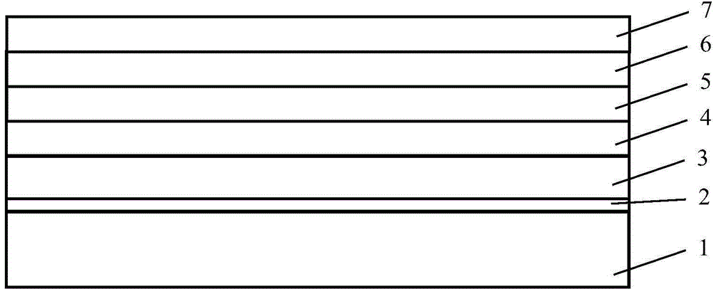
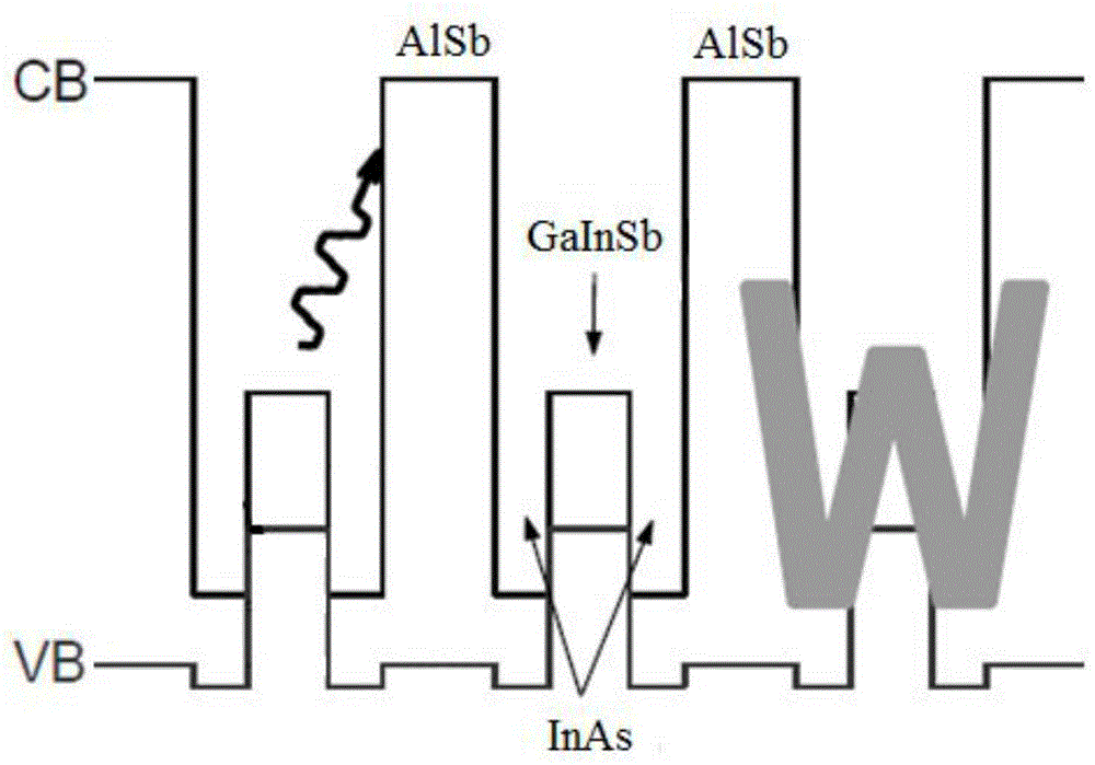
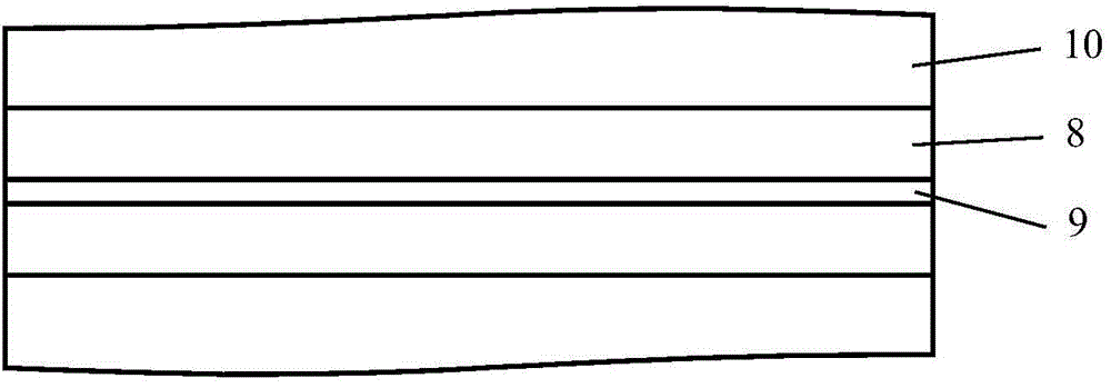
[0010] The W-type antimony-based semiconductor laser with gradually changing Ga In ratio of the present invention, from bottom to top, is GaSb substrate 1, GaSb buffer layer 2, P-type GaSb contact layer 3, P-type quantum well 4, intrinsic quantum well 5, N-type quantum well 6 and N-type InAs contact layer 7, such as figure 1 As shown, the P-type quantum well 4, the intrinsic quantum well 5, and the N-type quantum well 6 have a multi-period structure, and the structure of each single-period quantum well in the multi-period structure is composed of double InAs electron quantum wells 8 A sandwich structure sandwiching GaInSb hole quantum wells 9, the outer layer is a pair of AlSb alloy confinement layers 10, such as figure 2 , image 3 Shown; The GaInSb hole quantum well 9 is made of 3 layers of Ga 1-x In x Composition of Sb layer with 17ML thick Ga in the middle 0.8 In 0.2 Sb layer, level 1 is two 4ML thick Ga 0.9 In 0.1 Sb layer, Ga 1-x In x The total thickness of the...

Embodiment 2

[0012] The W-type antimony-based semiconductor laser with gradually changing Ga In ratio of the present invention, from bottom to top, is GaSb substrate 1, GaSb buffer layer 2, P-type GaSb contact layer 3, P-type quantum well 4, intrinsic quantum well 5, N-type quantum well 6 and N-type InAs contact layer 7, such as figure 1 As shown, the P-type quantum well 4, the intrinsic quantum well 5, and the N-type quantum well 6 have a multi-period structure, and the structure of each single-period quantum well in the multi-period structure is composed of double InAs electron quantum wells 8 A sandwich structure sandwiching GaInSb hole quantum wells 9, the outer layer is a pair of AlSb alloy confinement layers 10, such as figure 2 , image 3 Shown; The GaInSb hole quantum well 9 is made of 5 layers of Ga 1-x In x The Sb layer constitutes as Figure 4 shown, the middle is 17ML thick Ga 0.75 In 0.25 Sb layer, level 1 is two 2ML thick Ga 0.9 In 0.1 Sb layer, level 2 is two 2ML th...

Embodiment 3

[0014] The W-type antimony-based semiconductor laser with gradually changing Ga In ratio of the present invention, from bottom to top, is GaSb substrate 1, GaSb buffer layer 2, P-type GaSb contact layer 3, P-type quantum well 4, intrinsic quantum well 5, N-type quantum well 6 and N-type InAs contact layer 7, such as figure 1 As shown, the P-type quantum well 4, the intrinsic quantum well 5, and the N-type quantum well 6 have a multi-period structure, and the structure of each single-period quantum well in the multi-period structure is composed of double InAs electron quantum wells 8 A sandwich structure sandwiching GaInSb hole quantum wells 9, the outer layer is a pair of AlSb alloy confinement layers 10, such as figure 2 , image 3 Shown; The GaInSb hole quantum well 9 is made of 9 layers of Ga 1-x In x Composition of Sb layer with 17ML thick Ga in the middle 0.65 In 0.35 Sb layer, level 1 is two 1ML thick Ga 0.75 In 0.25 Sb layer, level 2 is two 1ML thick Ga 0.85 In...


PUM


Abstract

The invention relates to a W type antimony-based semiconductor laser with gradually varied Ga In proportion, which belongs to the technical field of semiconductor lasers. The existing InAs/GaInSb W type antimony-based semiconductor laser is difficult to realize luminescence at room temperature, and is less in output power of luminescence at low temperature (73K). The W type antimony-based semiconductor laser with gradually varied Ga In proportion sequentially comprises a GaSb substrate, a GaSb buffer layer, a P type GaSb contact layer, a P type quantum well, an intrinsic quantum well, an N type quantum well and an N type InAs contact layer from bottom to top, wherein the P type quantum well, the intrinsic quantum well and the N type quantum well respectively have a multi-period structure; the structure of each single-period quantum well in each multi-period structure is a sandwich structure that a GaInSb hole quantum well is clamped by double InAs electronic quantum wells; the outer layer is a pair of AlSb alloy limiting layers. The W type antimony-based semiconductor laser with gradually varied Ga In proportion is characterized in that the GaInSb hole quantum well is formed by 3 to 9 layers of Ga1-xInxSb layers, wherein x is equal to 0.05-0.35; the value of x of the Ga1-xInxSb layer in the middle is maximal; the Ga1-xInxSb layers on two sides are distributed in 1 to 4 levels from the middle to two sides; the values of x of two Ga1-xInxSb layers at the same level are the same, and the values of x of the Ga1-xInxSb layers from the middle to two sides are gradually reduced.

Description

technical field [0001] The invention relates to a W-type antimony-based semiconductor laser with a gradually changing GaIn ratio. During the growth process of the GaInSb layer, the GaIn ratio is gradually changed. Compared with the existing technology, the thickness of the GaInSb layer can be increased, thereby increasing the W-type antimony The output power of a base semiconductor laser belongs to the technical field of semiconductor lasers. Background technique [0002] Atmospheric monitoring and infrared imaging use the 2-5 μm band atmospheric window including 2-2.5 μm near-infrared and 3-5 μm mid-infrared. Therefore, this band is directly related to sensing technology, remote sensing, photoelectric countermeasures and other fields. The 2-5 μm band also contains many important molecular characteristic lines, and various molecular characteristic lines have their own characteristic absorption peaks. The above-mentioned molecules and their characteristic absorption peaks are...

Claims


Application Information

Patent Timeline
Patent Type & Authority Applications(China)
IPC IPC(8): H01S5/343
Inventor 唐吉龙魏志鹏方铉房丹高娴牛守柱王菲马晓辉王晓华
Owner CHANGCHUN UNIV OF SCI & TECH
Why Eureka
Try Eureka