Micro-current detection device for single-molecule conductance measurement system

A technology of conductance measurement and detection device, which is applied to measurement device, uses digital measurement technology to measure, changes range circuit and other directions, can solve problems such as conductance change, and achieve the effects of good linearity, large dynamic range and high sensitivity

Active Publication Date: 2015-05-27
ZHEJIANG NORMAL UNIVERSITY
View PDF7 Cites 11 Cited by
  • Summary
  • Abstract
  • Description
  • Claims
  • Application Information

AI Technical Summary

Problems solved by technology

[0006] The purpose of the present invention is to provide a micro-current detection system for single-molecule conductance measurement that can detect the rapidly changing weak current signal in the STM-BJ experiment, thereby effectively solving technical problems such as conductance changes in the scanning tunneling microscope split junction method experiment. device

Method used


Image

  • Micro-current detection device for single-molecule conductance measurement system
  • Micro-current detection device for single-molecule conductance measurement system
  • Micro-current detection device for single-molecule conductance measurement system

Examples


Embodiment 1

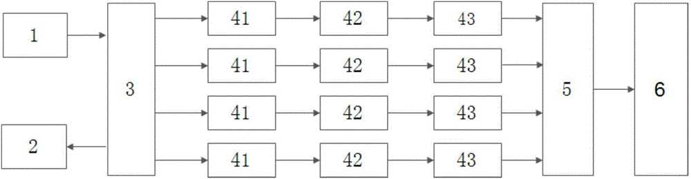
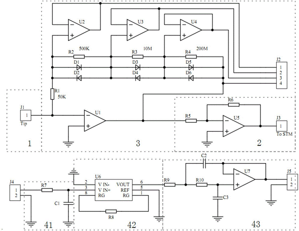
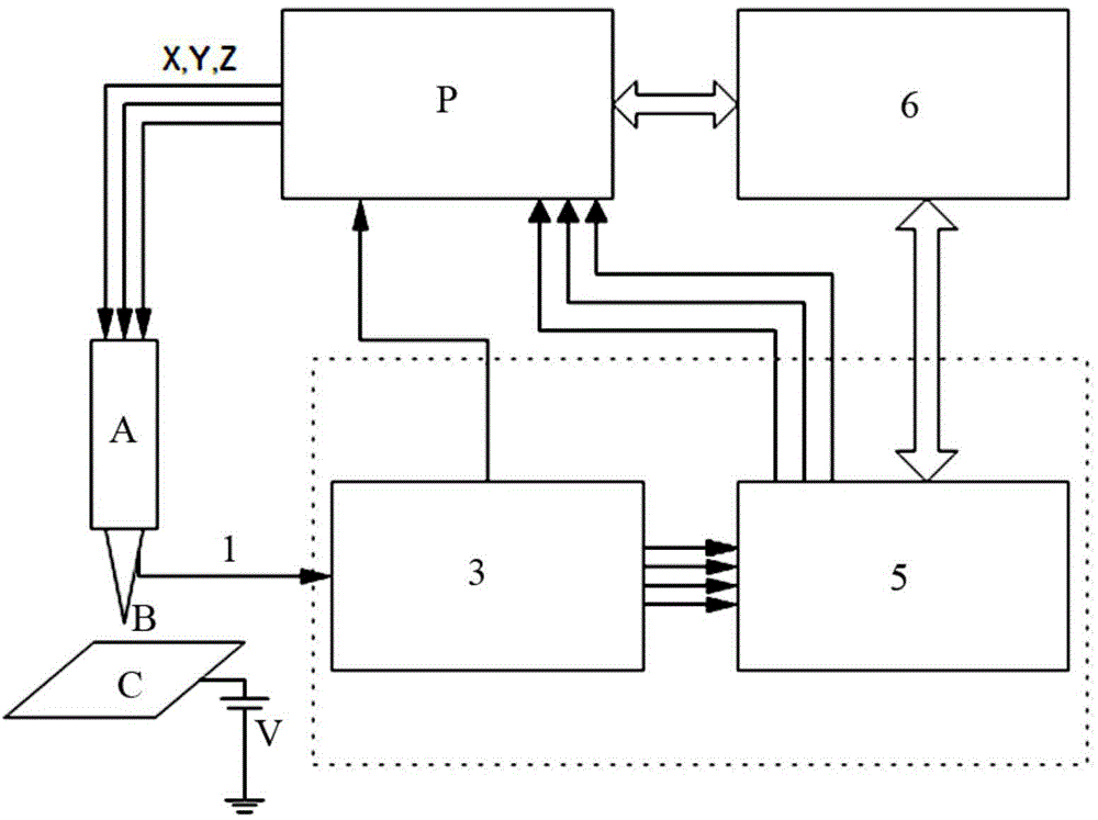
[0033] Take a piece of gold wire, cut it mechanically to make tip B, and assemble it into the scanning head with four-channel microcurrent amplifier; use Au(111) single crystal electrode as substrate C, soak substrate C in 1mM 4, The self-assembled film was formed in 4'-bipyridyl aqueous solution for 5 minutes, and then placed in the aqueous solution for 5 minutes to wash away excess molecules, dried and placed in the sample stage. First drive the motor so that the needle tip approaches the Au(111) substrate. After reaching the tunnel current region, the motor stops working. At this time, the piezoelectric ceramic tube of the scanning head starts to work. By changing the x, y and z directions added to the piezoelectric ceramic A The voltage can drive the tip B to move in three directions of x, y and z. When the mechanical and thermal drift of the whole device is almost negligible, keep the needle tip B and the substrate C at a bias voltage of 200mV (denoted as V), drive the ne...

Embodiment 2

[0035] Take a piece of gold wire, cut it mechanically to make a needle tip, and assemble it into a scanning head containing a four-channel microcurrent amplifier; use Au(111) single crystal electrode as the substrate, soak the substrate in 1mM 1,2-di The self-assembled film was formed in an aqueous solution of (4-pyridyl)ethylene for 5 minutes, and then soaked in an aqueous solution for 5 minutes to wash off excess molecules, and then put it into the sample stage after drying. First drive the motor so that the needle tip approaches the Au(111) substrate. After reaching the tunnel current region, the motor stops working. At this time, the piezoelectric ceramic tube of the scanning head starts to work. By changing the voltage applied to the piezoelectric ceramic in the x, y and z directions , which can drive the needle tip to move in the x, y and z directions. When the mechanical and thermal drift of the whole device is almost negligible, keep the needle tip and the substrate at...


PUM


Abstract

The invention relates to a micro-current detection device, in particular to a micro-current detection device for a single-molecule conductance measurement system. The micro-current detection device is provided with a see-saw circuit, a four-section current-voltage conversion circuit, pre-filter circuits, in-phase amplifying circuits, post-filter circuits and an optoelectronic isolation ADC acquisition card, wherein the four-section current-voltage conversion circuit is circumscribed with a shielded input tunnel current signal; the four-section current-voltage conversion circuit is output to an STM controller through the see-saw circuit to be used for imaging control; 4 paths of voltage signals of the four-section current-voltage conversion circuit after being subjected to current-voltage conversion sequentially pass through the pre-filter circuits, the in-phase amplifying circuits, the post-filter circuits and the four-channel optoelectronic isolation ADC data acquisition card clamped with an input port of a PC; the PC automatically judges the present current value calculated by selecting a voltage result at the same time through software. The micro-current detection device is wide in measuring range, self-adaptive, high in sensitivity, large in dynamic range and high in linearity.

Description

technical field [0001] The invention relates to a micro-current detection device, in particular to a micro-current detection device for a single-molecule conductance measurement system which is mainly applied to but not limited to a scanning tunneling microscope molecular conductance measurement system. Background technique [0002] With the development of split junction metal quantum conductance and single molecular junction conductance detection technologies such as scanning tunneling microscope split junction (STM-BJ) technology and mechanically controlled split junction (MCBJ) technology, researchers have begun to use this method to detect metal atoms Line conductance and single-molecule junction conductance, among which the scanning tunneling microscope split junction method (STM-BJ) is the most widely used. Usually, the scanning tunneling microscope molecular conductance measurement system is realized by transforming the commercialized scanning tunneling microscope: dr...

Claims


Application Information

Patent Timeline
Patent Type & Authority Applications(China)
IPC IPC(8): G01R19/25G01R15/09G01Q60/10
Inventor 周小顺郑菊芳梁景洪陈招斌
Owner ZHEJIANG NORMAL UNIVERSITY
Why Eureka
Try Eureka