Electron blocking layer structure of photoelectric device

A technology of electron blocking layer and photoelectric device, which is applied in the direction of electrical components, semiconductor devices, circuits, etc., can solve problems such as the decrease of hole injection efficiency and the increase of electron leakage probability, so as to improve the efficiency, reduce the migration potential energy, and improve the efficiency of electron holes. Compounding Efficiency Effect

Inactive Publication Date: 2015-05-27
西安利科光电科技有限公司
View PDF8 Cites 31 Cited by
  • Summary
  • Abstract
  • Description
  • Claims
  • Application Information

AI Technical Summary

Problems solved by technology

[0007] However, it is impossible for a single InAlGaN material to achieve a complete match between the lattice structure and the forbidden band width and the structure between the quantum well and the P layer through the adjustment of the In and Al components. Decreased hole injection efficiency and increased probability of electron leakage

Method used


Image

  • Electron blocking layer structure of photoelectric device
  • Electron blocking layer structure of photoelectric device
  • Electron blocking layer structure of photoelectric device

Examples


Embodiment Construction

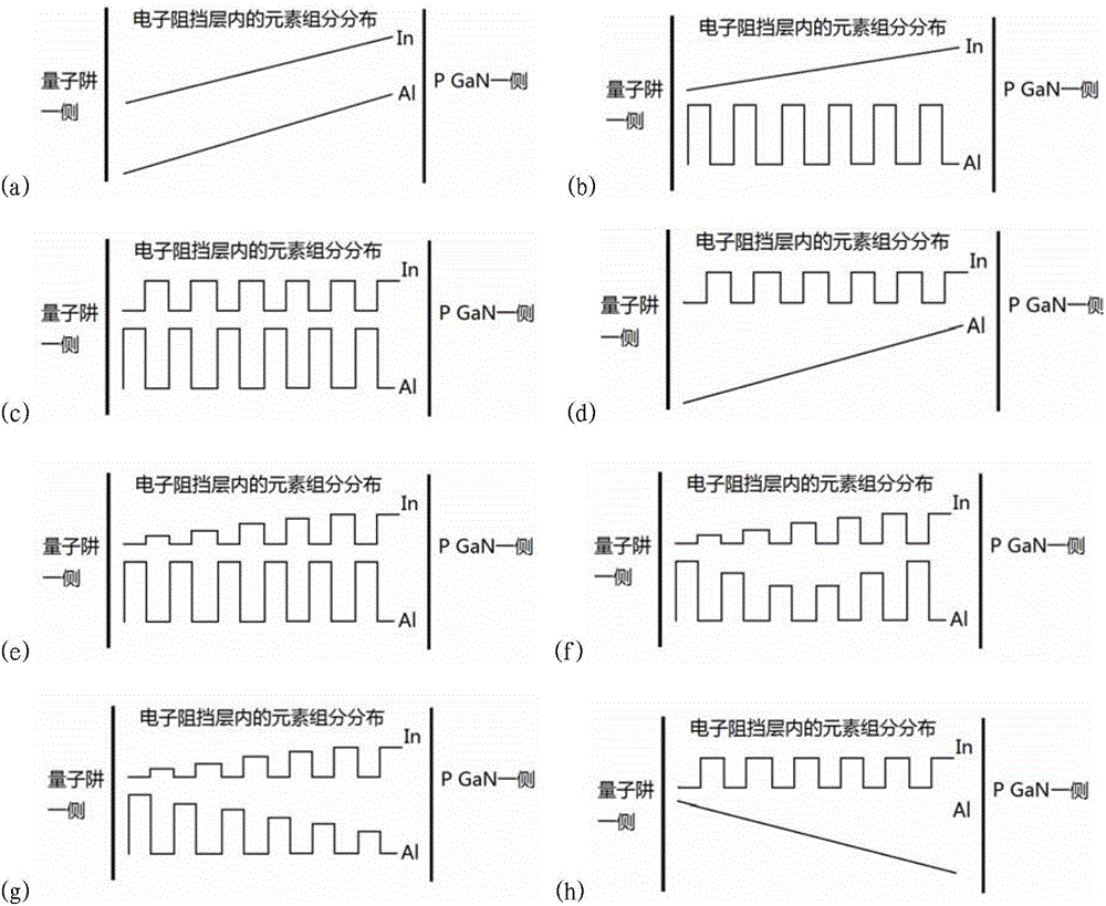
[0021] The electron blocking layer of the present invention is grown by AlInGaN or AlInGaN / InGaN superlattice structure (for example, 200 pairs), wherein the In component is ≤ 10%, and the Al component is ≤ 40%. There is a gradual distribution of In and Al components in the electron blocking layer, and the specific form is one of linear increase or decrease, step shape, concave shape, convex shape, parabolic shape or any combination of stages. image 3 Different example structures of Al and In components inside the electron blocking layer are given. The average data of the experimental results of each specific example structure is shown in Table 1 below, it can be seen that various embodiments of the present invention have achieved considerable benefits. It can be expected that with the further optimization of the experiment, the value will continue to improve; based on the concept of the present invention, refer to image 3 Proper deformation and combination optimization wil...


PUM


Abstract

The invention provides an electron blocking layer structure of a photoelectric device. The electron blocking layer structure is characterized in that structure matching between a quantum well and a P layer is achieved through adjusting a lattice structure and a band gap as much as possible; meanwhile, the formation of a polarized electric field is reduced, the formation of a negative charge area in an electron blocking layer is weakened as much as possible, and further the efficiency is improved; the electron leakage caused by energy band bending of the electron blocking layer and the increment of hole potential energy of the P layer are weakened. The electron blocking layer structure of the photoelectric device adopts AlInGaN or AlInGaN/InGaN super-lattice structure growth, wherein the In component is less than or equal to 10 percent; the Al component is less than or equal to 40 percent; the gradual distribution of the In component and the Al component exists in the electron blocking layer, and gradual change principles of the In component and the Al component are mutually independent; as for the electron blocking layer with an AlInGaN/InGaN super-lattice structure, the gradual change of the In component occurs in a super-lattice AlInGaN or a super-lattice AlInGaN/InGaN or in both the super-lattice AlInGaN and the super-lattice AlInGaN/InGaN.

Description

Technical field: [0001] The invention belongs to the technical field of photoelectric device design, and relates to a structural design of an electron blocking layer in an epitaxial structure of a photoelectric device. Background technique: [0002] In the prior art, a layer of AlGaN structure is inserted between the quantum well structure and P-type GaN as an electron-blocking layer (Electron-Blocking Layer: EBL for short) to block electrons from entering the P layer, thereby reducing device leakage and improving device efficiency. For the AlGaN resistive barrier layer, we have done a lot of research. For example, Chinese patent application 201110150996.0 "A LED structure using a graded electron blocking layer of aluminum composition" mentions an LED structure using a graded electron blocking layer of aluminum composition, in which the side that is in contact with the outer GaN barrier of the multi-quantum well layer Al with low Al composition x Ga 1-x N, 0≤x≤0.1, the si...

Claims


Application Information

Patent Timeline
Patent Type & Authority Applications(China)
IPC IPC(8): H01L33/14H01L33/04
CPCH01L33/04H01L33/145
Inventor 李淼黄宏嘉
Owner 西安利科光电科技有限公司
Why Eureka
Try Eureka