

Field-programmable gate array testing method
A test method and gate array technology, applied in the field of microelectronics, can solve the problem of low test accuracy and validity of field programmable gate array chips
- Summary
- Abstract
- Description
- Claims
- Application Information
AI Technical Summary
Problems solved by technology
Method used
Image

Examples
Embodiment 1
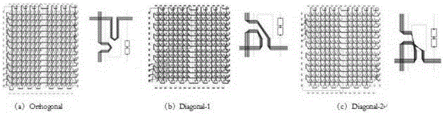
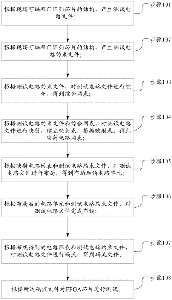
[0039] Step 201: According to the function of the test circuit and the structure of the FPGA chip to be tested, the test circuit file is generated. In the embodiment of the present invention, the test circuit file includes the description of the logic unit test circuit inside the VS1000FPGA, the description of the input and output unit test circuit, General wiring resource test circuit description and global wiring resource test circuit description, wherein, the logic unit test circuit includes all the working modes of the unit, the input and output unit test circuit includes all the attributes of the unit, and the general wiring resource test circuit includes The wiring rules of wiring and switch boxes, the global wiring resource test circuit includes the wiring rules of all global wiring branches;
[0040] Step 202: According to the structure of the field programmable gate array chip, generate a test circuit constraint file; in practice, it is also necessary to consider the f...
PUM
 Abstract
Description
Claims
Application Information