Composite fast recovery diode and preparation method thereof

A recovery diode and manufacturing method technology, applied in semiconductor/solid-state device manufacturing, electrical components, circuits, etc., can solve problems such as poor consistency of on-state voltage drop, long reverse recovery time, and device reliability decline, and achieve UIS improvement , Reduce the recovery time, reduce the effect of on-state pressure drop

Active Publication Date: 2015-06-17
MACMIC SCIENCE & TECHNOLOGY CO LTD
View PDF4 Cites 12 Cited by
  • Summary
  • Abstract
  • Description
  • Claims
  • Application Information

AI Technical Summary

Problems solved by technology

However, because the device is a bipolar device, the reverse recovery time is long, and most of them use heavy metal doping technology to control the minority carrier lifetime, resulting in poor consistency of on-state voltage drop and poor current sharing characteristics. high
[0005] Furthermore, the current PIN diode has no N-type charge accumulation region structure. During the reverse recovery process of the PIN junction diode, the carriers are quickly extracted from the base region, and the second avalanche electric field formed at the N-N+ junction is easily increased. , resulting in a decrease in UIS capability and a decrease in device reliability

Method used


Image

  • Composite fast recovery diode and preparation method thereof
  • Composite fast recovery diode and preparation method thereof

Examples


Embodiment Construction

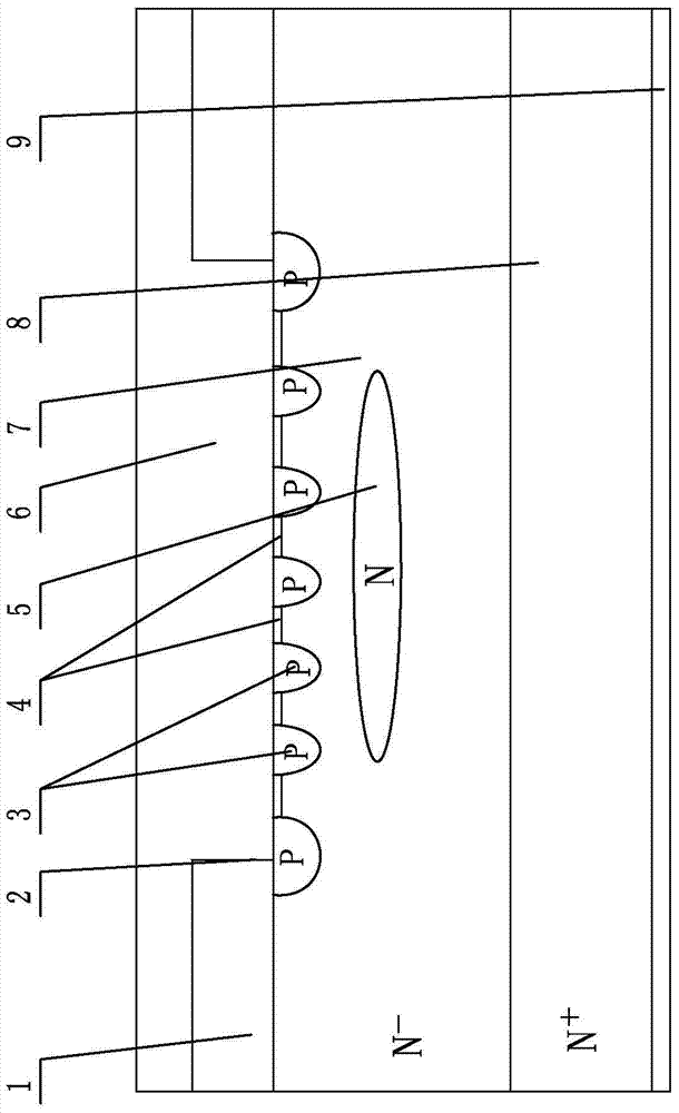
[0029] See figure 1 Shown, the preparation method of composite fast recovery diode of the present invention,

[0030] (1) Oxidation and lithography active area: After cleaning the silicon wafer with epitaxial layer, perform oxidation treatment to form a field oxide layer on the front side of the silicon wafer, and then photoetch and etch the active area on the front side of the silicon wafer window, the silicon wafer is an N+ type substrate silicon wafer.

[0031] (2) N-type impurity ion implantation: use an ion implanter to implant N-type impurity ions into the active area, the implantation energy is: 100-500kev, and the implantation dose is 1E12-5E14cm -2 .

[0032] (3) N push junction: Put the silicon wafer into a high-temperature diffusion furnace to push the N-type impurity ions to form a charge accumulation region. The concentration of N-type impurity ions in the charge accumulation region is higher than that of the epitaxial layer. , the junction depth of the N-type ...


PUM

PropertyMeasurementUnit
thicknessaaaaaaaaaa
thicknessaaaaaaaaaa

Abstract

The invention relates to a preparation method for a composite fast recovery diode. The method comprises the steps that 1, an active area is subjected to oxidization and photoetching; 2, N-typed impurity ions are injected; 3, N knot pushing is conducted; 4, P-area injection windows are formed; 5, P-typed impurity ions are injected; 6, knot pushing is conducted; 7, Schottky areas are formed; 8, metal film deposition is conducted; 9, back reduction is conducted; 10, back metallization is conducted to obtain the composite fast recovery diode. The composite fast recovery diode has the advantages that the forward voltage drop consistence is good, the avalanche tolerance capacity is high and the recovery property is good.

Description

technical field [0001] The invention relates to a composite fast recovery diode and a preparation method thereof, belonging to the technical field of fast recovery diodes. Background technique [0002] At present, fast recovery diodes with soft recovery characteristics are produced, and their active regions are generally integral Schottky structures or PIN structures. [0003] Simple Schottky diodes have the advantages of small on-state voltage drop, good consistency, and fast reverse recovery time trr because they are multiple sub-devices, but they also have low breakdown voltage (up to 300V) and large leakage current at high temperature. , Poor avalanche tolerance UIS ability, weak anti-static discharge ESD ability and other shortcomings. [0004] The PIN diode has the advantages of small on-state voltage drop, high breakdown voltage, good avalanche withstand UIS capability, strong anti-static discharge ESD capability, and small high-temperature leakage. However, because...

Claims


Application Information

Patent Timeline
Patent Type & Authority Applications(China)
IPC IPC(8): H01L21/329H01L29/861H01L29/06
Inventor 林茂张景超戚丽娜刘利峰赵善麒王晓宝
Owner MACMIC SCIENCE & TECHNOLOGY CO LTD
Why Eureka
Try Eureka