Using charge coupling to realize voltage-resistant power mos device and preparation method thereof

A MOS device and charge-coupled technology, applied in electrical components, semiconductor devices, circuits, etc., can solve the problems of small resistivity, influence, and low on-resistance of epitaxial silicon materials

Active Publication Date: 2017-09-05
WUXI NCE POWER
View PDF6 Cites 0 Cited by
  • Summary
  • Abstract
  • Description
  • Claims
  • Application Information

AI Technical Summary

Problems solved by technology

[0005] When the above-mentioned structure withstands voltage, the PN junction in the withstand voltage protection zone will be depleted, and the depleted area will gradually connect together laterally with the increase of voltage to support the electric field. The number of field limiting rings 39 determines the level of withstand voltage At the same time, the concentration, junction depth, and spacing of the field limiting ring 39 are all determined according to the concentration of the drift region forming the PN junction with it. Therefore, a specific process flow is required to manufacture the field limiting ring 39, and it is easily affected by other processes. Affected, resulting in the withstand voltage stability and reliability of the device are susceptible to fluctuations
[0006] In addition, for some semiconductor devices, the cells in the active region adopt a capacitive plate structure, which can realize charge coupling. When the coupled charge is balanced with the charge in the surrounding drift region, the depletion region formed by the two charges It can support the withstand voltage. Compared with traditional power devices, the resistivity of the epitaxial silicon material used in this type of device is smaller, which can obtain lower on-resistance. In order to meet higher requirements, the number of field limiting rings 39 needs to be more, and the process tolerance is smaller, which is not conducive to the reliability and cost performance of this type of advanced devices.

Method used


Image

  • Using charge coupling to realize voltage-resistant power mos device and preparation method thereof
  • Using charge coupling to realize voltage-resistant power mos device and preparation method thereof
  • Using charge coupling to realize voltage-resistant power mos device and preparation method thereof

Examples


Embodiment Construction

[0062] The present invention will be further described below in conjunction with specific drawings and embodiments.

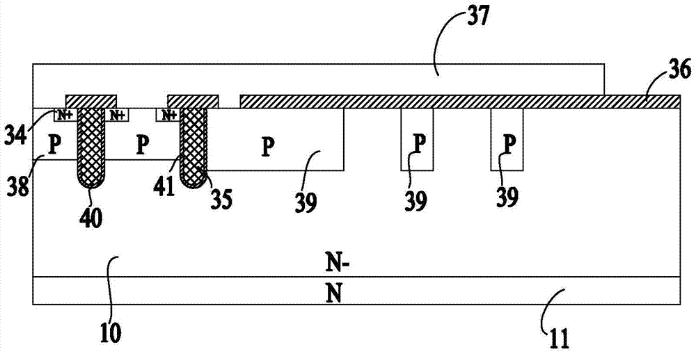
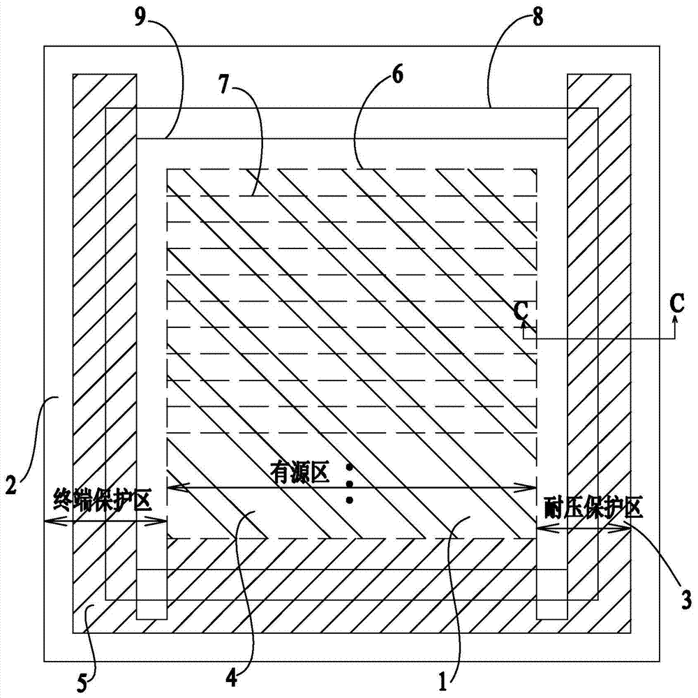
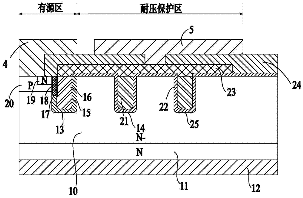
[0063] Such as figure 2 and image 3 As shown: In order to improve the withstand voltage capability and high withstand voltage reliability, and reduce the proportion of the entire chip area occupied by the terminal protection area, taking the N-type power MOS device as an example, the present invention includes the power MOS device located on the top view plane of the power MOS device. The active area 1 and the terminal protection area 2 of the semiconductor substrate, the active area 1 is located in the central area of ​​the semiconductor substrate, the terminal protection area 2 is located at the outer circle of the active area 1 and surrounds the active area 1, and the terminal protection The region 2 includes a withstand voltage protection region 3 adjacent to the active region 1; on the cross section of the power MOS device, the semiconductor substrate i...


PUM


Abstract

The invention relates to a power MOS device capable of achieving voltage resistance by charge coupling and a preparation method thereof. The device is characterized in that a connected voltage resisting ring is of a groove structure; a connected voltage resisting groove is filled with voltage-resistant conductive polycrystalline silicon; an active area includes a plurality of active cells; grid electrode conductive polycrystalline silicon is in contact with the sidewall of an active cell groove through an insulated grid oxide layer and is isolated from cell conductive polycrystalline silicon and a cell insulated oxide layer through the insulated grid oxide layer; the bottom part of the grid electrode conductive polycrystalline silicon is positioned below a second conductive type well region; a first conductive type injection area and the second conductive type well region are both in contact with active area metal ohm on the first main surface of the active area; metal in the active area is electrically connected with metal in a voltage resisting area; the cell conductive polycrystalline silicon is kept at equal potential with the voltage resisting conductive polycrystalline silicon. The device is high in voltage resistance and high in voltage resisting reliability; in addition, a terminal protection area occupies a little area of the whole chip area; the device is suitable for mass production.

Description

technical field [0001] The invention relates to a power MOS device and a preparation method thereof, in particular to a power MOS device and a preparation method thereof which utilize charge coupling to realize voltage resistance, and belongs to the technical field of power MOS devices. Background technique [0002] Semiconductor power devices usually need to withstand a certain voltage, ranging from tens of volts to thousands of volts, and the two major factors to achieve the withstand voltage of the device are the material used in the device and the structure of the device. At present, the most widely used semiconductor power device is a silicon device. The material used is silicon material, usually epitaxial silicon material, which has a specific resistivity and thickness; and the structure of the device includes an active region structure and a terminal protection region structure. , the former is usually the area where the current flows when the device is turned on, and...

Claims


Application Information

Patent Timeline
Patent Type & Authority Patents(China)
IPC IPC(8): H01L29/78H01L29/06
CPCH01L29/0657H01L29/78
Inventor 朱袁正叶鹏
Owner WUXI NCE POWER
Why Eureka
Try Eureka