Thin film transistor and manufacturing method thereof as well as array substrate and display device

A technology of a thin film transistor and a manufacturing method, applied in the field of semiconductor device preparation, capable of solving problems such as easy disconnection of pixel electrodes 5, increased production costs, uneven thickness, etc., and achieving problems of easy disconnection, improved yield, and uniform thickness Effect

Active Publication Date: 2015-06-17
BOE TECH GRP CO LTD
View PDF4 Cites 11 Cited by
  • Summary
  • Abstract
  • Description
  • Claims
  • Application Information

AI Technical Summary

Problems solved by technology

When coplanar TFT is used in TFT-LCD, for top gate coplanar TFT, such as figure 1 As shown, the pixel electrode 5 is in electrical contact with the drain electrode 4 through the via hole penetrating the passivation layer 102 and the gate insulating layer 101. Since the depth of the via hole is too large, it is difficult to climb the slope, and the pixel electrode 5 is easily disconnected, causing electrical contact. poor sexual contact
However, if the electrical connection between the pixel electrode 5 and the drain electrode 4 is realized in the form of a jumper, the number of Masks will be increased, and the production cost will be increased.
For the bottom gate coplanar TFT, such as figure 2 As shown, the active layer 2 overlaps the source electrode 3 and the drain electrode 4, and the etching process for forming the source electrode 3 and the drain electrode 4 results in rough sides of the source and drain metal. Since the thickness of the active layer 2 is very thin, when When it is lapped on the source electrode 3 and the drain electrode 4, the sides of the source electrode 3 and the drain electrode 4 are rough and climb, which makes the active layer 2 easy to break, and the thickness is uneven, and it is easy to shock during the power-on process. short circuit

Method used


Image

  • Thin film transistor and manufacturing method thereof as well as array substrate and display device
  • Thin film transistor and manufacturing method thereof as well as array substrate and display device
  • Thin film transistor and manufacturing method thereof as well as array substrate and display device

Examples


Embodiment Construction

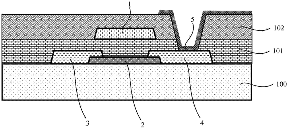
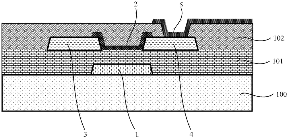
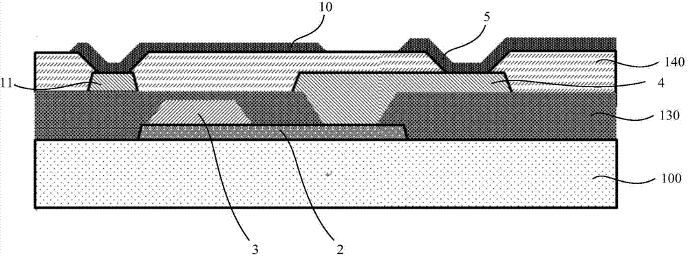
[0028] The invention provides a thin film transistor, the source electrode and the drain electrode of which are located on the active layer, and the entire active layer is located in the same plane, so that the active layer does not have the problem of easy disconnection caused by climbing difficulties, and the active layer The thickness is uniform, and the phenomenon of breakdown and short circuit is not easy to occur in the working process, which improves the yield rate of the thin film transistor. Furthermore, the source electrode and the drain electrode are arranged in a non-same-layer structure, so that the distance between the source electrode and the drain electrode can be flexibly adjusted, and it is easier to realize a narrow channel and improve the performance of the thin film transistor.

[0029] For a liquid crystal display device, the electrode on the array substrate electrically contacting the drain electrode of the thin film transistor is a transparent pixel elec...


PUM


Abstract

The invention relates to the technical field of semiconductor manufacturing, and discloses a thin film transistor and a manufacturing method thereof as well as an array substrate and a display device. A source electrode and a drain electrode of the thin film transistor are located on an active layer, the whole active layer is located on a same plane, the problem that a wire of the active layer is easy to break due to climbing difficulty in the prior art is solved, the thickness of the active layer is uniform, the breakdown short circuit phenomenon cannot occur, and the yield of the thin film transistor is improved. The source electrode and the drain electrode are arranged to be in a different layer structure, the distance between the source electrode and the drain electrode can be flexibly adjusted, a narrow channel is easy to realize, and the performance of the thin film transistor is improved.

Description

technical field [0001] The invention relates to the technical field of semiconductor device preparation, in particular to a thin film transistor and a manufacturing method thereof, an array substrate and a display device. Background technique [0002] combine figure 1 and figure 2 As shown, in a coplanar thin film transistor (Thin Film Transistor, TFT for short), the source electrode 3 , the drain electrode 4 and the gate electrode 1 are all disposed on the same side of the active layer 2 . According to the position of the gate electrode 1 relative to the active layer 2, coplanar TFTs are classified into top-gate coplanar TFTs (combined figure 1 shown) and bottom-gate coplanar TFT (combined figure 2 shown). [0003] Thin Film Transistor Liquid Crystal Display (TFT-LCD for short) has the characteristics of small size, low power consumption, no radiation, and relatively low manufacturing cost, and occupies a dominant position in the current flat panel display market. Wh...

Claims


Application Information

Patent Timeline
Patent Type & Authority Applications(China)
IPC IPC(8): H01L29/786H01L29/06H01L29/417H01L21/336H01L27/12
CPCH01L27/1214H01L29/06H01L29/41733H01L29/66742H01L29/786H01L29/40114H01L29/66969H01L29/7869H01L27/1288H01L29/42384H01L21/0274H01L29/78606H01L29/78618H01L29/78696
Inventor 张立
Owner BOE TECH GRP CO LTD
Why Eureka
Try Eureka