

Adhesive film, dicing/die-bonding film, method for manufacturing semiconductor device, and semiconductor device
A technology of die-bonding film and manufacturing method, which is applied in the direction of film/sheet adhesive, semiconductor/solid-state device manufacturing, semiconductor device, etc., can solve the coating amount of paste adhesive, coating shape deviation, It is difficult to homogenize and requires special equipment to achieve the effect of improving yield, good production efficiency, and preventing communication speed from being reduced.
- Summary
- Abstract
- Description
- Claims
- Application Information
AI Technical Summary
Problems solved by technology
Method used
Image

Examples
no. 1 approach
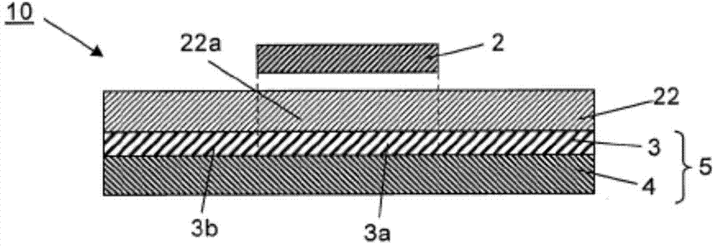
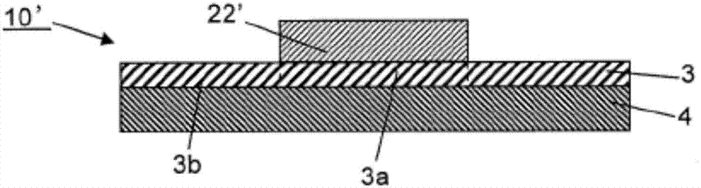
[0073] In the first embodiment, if figure 1 As shown, the following description will be made by taking, as an example, the form of a dicing / die-bonding film in which an adhesive film 22 for embedding is laminated on a dicing film 5 in which an adhesive layer 3 is laminated on a substrate 4. made. In this embodiment mode, a mode in which the electrical connection between the adherend and the first semiconductor element is realized by wire bonding connection will be described.
[0074] Adhesive film
[0075] In the adhesive film 22, the dielectric constant at 1 MHz after thermosetting is set to 4.00 or less. The dielectric constant is preferably 3.50 or less, more preferably 3.00 or less. By setting the dielectric constant after thermosetting within such a range, charges such as ions and polar functional groups that may cause corrosion of the first semiconductor element and connection structure (bonding wires, surface electrodes, etc.) in the semiconductor device can be su...
no. 2 approach
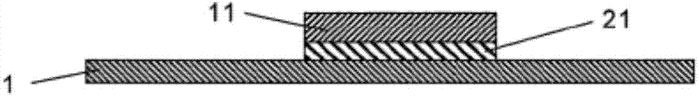
[0208] In the first embodiment, the step of fixing the first semiconductor element to the adherend is performed by bonding the film, and the electrical connection between the two is realized by wire bonding. 1 The flip-chip connection of the protruding electrodes of the semiconductor element is used to realize the fixation and electrical connection between the two. Therefore, since the second embodiment differs from the first embodiment only in the fixing method in the first fixing step, the difference will be mainly described below.
[0209] 1st fixed process
[0210] In this embodiment, in the aforementioned first fixing step, the first semiconductor element 41 is fixed to the adherend 1 by flip-chip connection (see Figure 4A ). In the flip-chip connection, the circuit surface of the first semiconductor element 41 faces the adherend 1, so-called face-down mounting. A plurality of protruding electrodes 43 such as bumps are provided on the first semiconductor element 41 ...
Embodiment approach
[0220] In the first embodiment, the second semiconductor element 12 is produced through a dicing process using a dicing die-bonding film and a picking process. Furthermore, the first semiconductor element 11 can also be produced using a dicing / die-bonding film in the same manner. At this time, a semiconductor wafer for cutting out the first semiconductor element 11 is separately prepared, and then the first semiconductor element 11 is fixed to the adherend 1 through the above-mentioned wafer bonding step, dicing step, and pickup step. The third semiconductor element 13 and semiconductor elements stacked thereon can also be produced in the same manner.
[0221] When three-dimensionally mounting a semiconductor element on an adherend, a buffer coat film may be formed on one side on which a circuit of the semiconductor element is formed. Examples of the buffer coat film include silicon nitride films and films made of heat-resistant resins such as polyimide resins.
[0222] In e...
PUM
| Property | Measurement | Unit |
|---|---|---|
| The average particle size | aaaaa | aaaaa |
| Storage modulus | aaaaa | aaaaa |
| Melt viscosity | aaaaa | aaaaa |
Abstract
Description
Claims
Application Information