GaN-based laser with asymmetric Al component AlGaN limiting layers

A GaN-based, confinement layer technology, applied in lasers, laser parts, semiconductor lasers, etc., can solve problems such as severe, increased tensile stress, and warpage of GaN homogenous substrates

Active Publication Date: 2015-06-24
INST OF SEMICONDUCTORS - CHINESE ACAD OF SCI
View PDF6 Cites 11 Cited by
  • Summary
  • Abstract
  • Description
  • Claims
  • Application Information

AI Technical Summary

Problems solved by technology

However, the tensile stress in the AlGaN confinement layer with high Al composition becomes larger, which makes the warping problem of GaN homogeneous substrate more serious

Method used


Image

  • GaN-based laser with asymmetric Al component AlGaN limiting layers
  • GaN-based laser with asymmetric Al component AlGaN limiting layers
  • GaN-based laser with asymmetric Al component AlGaN limiting layers

Examples


Embodiment Construction

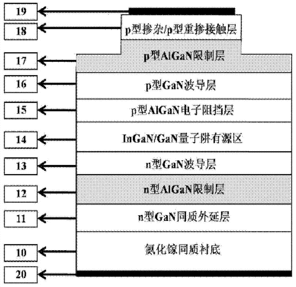
[0025] see figure 1 As shown, the present invention provides a gallium nitride-based laser with an asymmetric Al composition AlGaN confinement layer, comprising:

[0026] A gallium nitride homogeneous substrate 10, the gallium nitride homogeneous substrate 10 is an n-type doped self-supporting gallium nitride material with a thickness of 200-1000 μm;

[0027] An n-type GaN homoepitaxial layer 11, which is fabricated on a gallium nitride homogeneous substrate 10, the n-type GaN homoepitaxial layer is n-type GaN doped with Si, with a thickness of 1-10 μm;

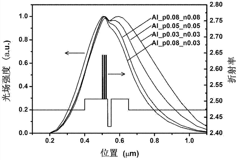
[0028] An n-type AlGaN confinement layer 12, which is fabricated on the n-type GaN homoepitaxial layer 11, the n-type AlGaN confinement layer 12 is Si-doped n-type AlGaN, the Al composition is 0.01-0.1, and the thickness is 0.2-1 μm ;

[0029] An n-type GaN waveguide layer 13, which is fabricated on the n-type AlGaN confinement layer 12, the n-type GaN waveguide layer is Si-doped n-type GaN with a thickness of 50-300 μm;

...


PUM


Abstract

A GaN-based laser with asymmetric Al component AlGaN limiting layers comprises a GaN native substrate, an n-type GaN homoepitaxial layer, the n-type AlGaN limiting layer, an n-type GaN waveguide layer, an InGaN / lGaN quantum well active region, a p-type AlGaN electron blocking layer, a p-type GaN waveguide layer, the p-type AlGaN limiting layer, a p-type doped / p-type heavily-doped contact layer, a p-type ohmic electrode and an n-type ohmic electrode. The n-type GaN homoepitaxial layer is manufactured on the GaN native substrate, the n-type AlGaN limiting layer is manufactured on the n-type GaN homoepitaxial layer, the n-type GaN waveguide layer is manufactured on the n-type AlGaN limiting layer, the InGaN / lGaN quantum well active region is manufactured on the n-type GaN waveguide layer, the p-type AlGaN electron blocking layer is manufactured on the InGaN / lGaN quantum well active region, the p-type GaN waveguide layer is manufactured on the p-type AlGaN electron blocking layer, the p-type AlGaN limiting layer is manufactured on the p-type GaN waveguide layer, a protruding ridge is formed in the middle of the p-type AlGaN limiting layer, the p-type doped / p-type heavily-doped contact layer is manufactured on the protruding ridge of the p-type AlGaN limiting layer, the p-type ohmic electrode is manufactured on the p-type doped / p-type heavily-doped contact layer, and the n-type ohmic electrode is manufactured on the lower surface of the GaN native substrate.

Description

technical field [0001] The invention relates to the field of semiconductor optoelectronic devices, in particular to a GaN-based laser with an asymmetrical Al composition AlGaN confinement layer. Background technique [0002] In semiconductor lasers, the distribution of optical field and absorption loss are the key factors affecting the laser threshold and output power. In the traditional gallium nitride laser structure, there are n-type and p-type waveguides and confinement layers on the upper and lower sides of the active region, and the n-type and p-type AlGaN confinement layers confine most of the optical field in the waveguide. However, there will still be a small part of the optical field extending into the AlGaN confinement layer, and even extending to the metal electrode regions on both sides of the laser. GaN and AlGaN materials have strong absorption caused by free carrier absorption and impurity absorption for light with a wavelength greater than the interband tra...

Claims


Application Information

Patent Timeline
Patent Type & Authority Applications(China)
IPC IPC(8): H01S5/343
Inventor 陈平赵德刚朱建军刘宗顺江德生杨辉
Owner INST OF SEMICONDUCTORS - CHINESE ACAD OF SCI
Why Eureka
Try Eureka