A scanning probe and its manufacturing method

A scanning probe and manufacturing method technology, applied in scanning probe technology, scanning probe microscopy, measuring device and other directions, can solve problems such as high cost and complicated process, and achieve increased wear resistance, simple process method, high-resolution effects

Active Publication Date: 2017-09-29
INST OF SEMICONDUCTORS - CHINESE ACAD OF SCI
View PDF5 Cites 0 Cited by
  • Summary
  • Abstract
  • Description
  • Claims
  • Application Information

AI Technical Summary

Problems solved by technology

However, the entire probe is made entirely of diamond, which is complicated in process and high in cost.

Method used


Image

  • A scanning probe and its manufacturing method
  • A scanning probe and its manufacturing method
  • A scanning probe and its manufacturing method

Examples


Embodiment Construction

[0035] In this example, the base of the probe is 3.4mm long, 1.6mm wide, and the tip height is about 4um. The microcantilever is 200um long, 30um wide, and 4um thick. The method of making the scanning probe is as follows: Figure 1a ~ Figure 1h As shown, the specific process flow is as follows:

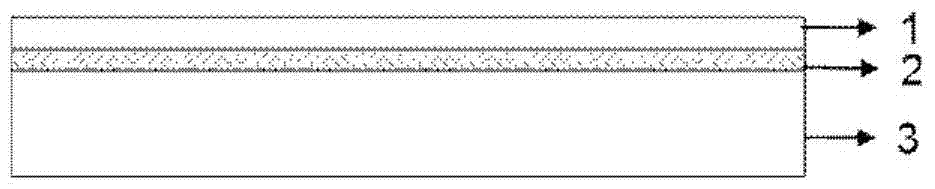
[0036] Step 1: adopt (100) oriented N-type SOI silicon wafer as the substrate for preparing the high-resolution, high-sensitivity, high-reliability scanning probe device, the substrate is composed of top layer silicon 1, buried oxide layer 2 and Bulk silicon 3, wherein the thickness of the top silicon is the sum of the height of the needle tip and the thickness of the micro-cantilever beam, that is, 8um, the thickness of the buried oxide layer is 1um, and the thickness of the bulk silicon is 400um, such as Figure 1a shown.

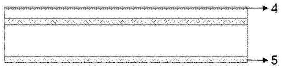
[0037] Step 2: Thermally oxidize the SOI sheet at 1000°C to form a thin silicon dioxide layer 4 with a thickness of about 300nm, which is used as a mask when e...


PUM

PropertyMeasurementUnit
thicknessaaaaaaaaaa

Abstract

The invention discloses a high-resolution, high-sensitivity and high-reliability scanning probe fabrication method. The method is realized by the micro-nano processing technology, that is, the needle tip and the cantilever beam are fabricated on the substrate by photolithography and etching, the needle tip is sharpened by low temperature oxidation technology, and the local diamond film is deposited on the needle tip by using a shadow mask. The invention combines the conventional micro-nano processing method with the diamond film local deposition technology, realizes the high resolution, high sensitivity and high reliability of the probe, reduces the cost, and is suitable for mass production.

Description

technical field [0001] The invention relates to the field of MEMS (micro-electromechanical system) manufacturing and engineering, in particular to a high-resolution, high-sensitivity, high-reliability scanning probe and a manufacturing method thereof. Background technique [0002] In 1986, the atomic force microscope (AFM) was born, which realized the atomic-level observation of the surface of conductors, semiconductors and insulator materials. AFM uses the interaction force between the needle tip and the sample to detect the topography of the sample surface. It has no requirement for the conductivity of the sample. It is widely used in multidisciplinary fields such as biology, chemistry, and materials. It is a very important surface imaging tool. [0003] In the atomic force microscope, the probe is one of its core components, which directly determines the quality of the atomic force microscope imaging. The AFM probe consists of a micro-cantilever beam and a needle tip fix...

Claims


Application Information

Patent Timeline
Patent Type & Authority Patents(China)
IPC IPC(8): G01Q60/38
Inventor 杨晋玲何欢张金英杨富华
Owner INST OF SEMICONDUCTORS - CHINESE ACAD OF SCI
Why Eureka
Try Eureka