
Optical filter and manufacturing method thereof, touch liquid crystal display and manufacturing method thereof

A production method and filter technology, which are applied in the fields of filters, optics, instruments, etc., can solve the problems such as the requirements for the alignment accuracy of lamination, the thickness of the finished product, and the difficulty of the process, so as to avoid the alignment accuracy, improve the The effect of high rate and cost reduction

Active Publication Date: 2017-07-11
INESA DISPLAY MATERIALS
View PDF7 Cites 0 Cited by
  • Summary
  • Abstract
  • Description
  • Claims
  • Application Information

AI Technical Summary

Problems solved by technology

[0019] However, among the above-mentioned four structures, the first three structures separately manufacture the LCD and the touch screen, and then integrate them together, so the process is complicated, the cost is high, the finished product is thick, and the alignment accuracy is required; the fourth existing The process is relatively complicated, and it is necessary to make sensing and driving ITO electrodes in the original liquid crystal cell. There are many processes, the process is difficult, the yield rate is low, and the cost is also high.

Method used


Image

  • Optical filter and manufacturing method thereof, touch liquid crystal display and manufacturing method thereof
  • Optical filter and manufacturing method thereof, touch liquid crystal display and manufacturing method thereof
  • Optical filter and manufacturing method thereof, touch liquid crystal display and manufacturing method thereof

Examples


Embodiment Construction

[0053] As mentioned in the background art section, touch LCDs with mainstream structures in the prior art generally have disadvantages such as complicated structure and process, high cost, long production cycle, and low production yield, and the most important thing is that they are thick.

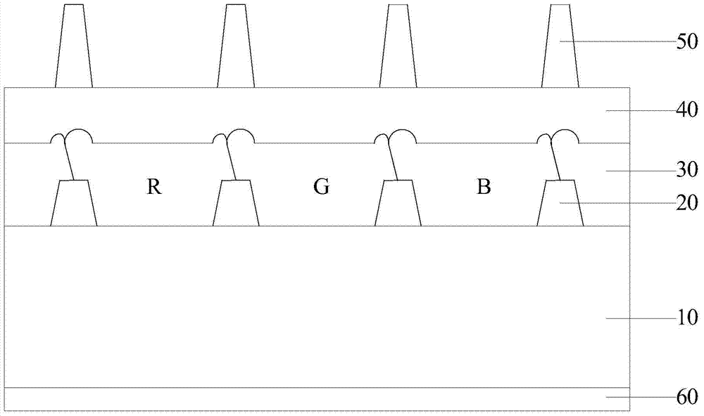
[0054] In view of the above problems, the present invention provides an optical filter integrated with a touch function and a manufacturing method thereof. The photoresist unit in the photoresist layer includes at least four kinds of photoresist, which changes the materials and materials of the two photoresist in the photoresist layer. A structure such that at least some of the first photoresists arranged along at least some of the same first directions are connected together and have conductivity, and at least some of the third photoresists arranged along at least some of the same second directions are connected together and have The second photoresist and the fourth photoresist are used t...


PUM

PropertyMeasurementUnit
electrical conductivityaaaaaaaaaa
thicknessaaaaaaaaaa
thicknessaaaaaaaaaa

Abstract

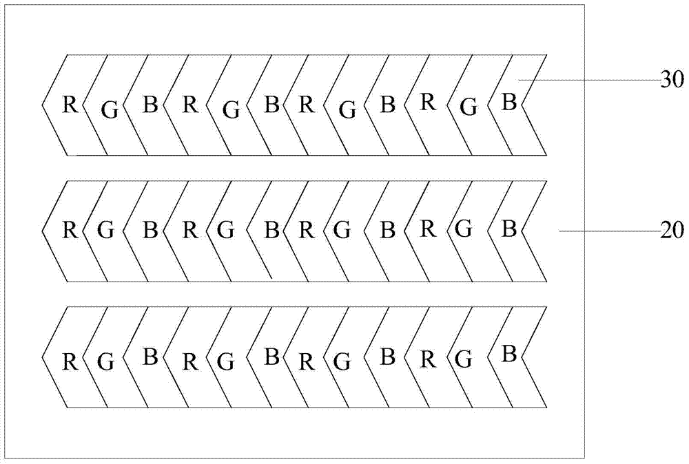
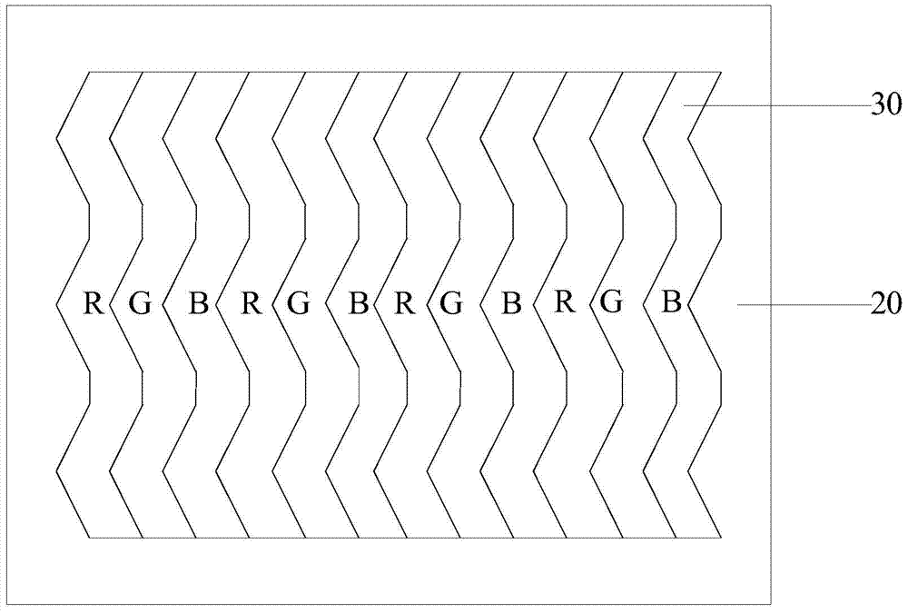
Provided is an optical filter and a manufacturing method, as well as a touch liquid crystal display and a manufacturing method. The optical filter comprises a substrate, a black matrix, a light resistance layer, and a flat layer. The black matrix is located on the substrate and is in a net structure; and the black matrix has gaps and is exposed outside the surface of the substrate. The light resistance layer comprises a plurality of light resistance units; each light resistance unit comprises at least first light resistors, second light resistors, third light resistors, and fourth light resistors. The first light resistors, the second light resistors, the third light resistors and the fourth light resistors are at least located inside the gaps on the surface of the substrate. All or parts of the first light resistors distributed completely or partially along the same first directions are connected together and are of conductivity. All or parts of the third light resistors distributed completely or partially along the same second directions are connected together and are of conductivity. The second light resistors and the fourth light resistors are used for isolating the adjacent first light resistors and third light resistors. The flat layer is located above the light resistance layer. With the simplified structure and technology, the production cycle can be shortened, and the production yield can be increased, accordingly the touch liquid crystal display can be thinner.

Description

technical field [0001] The invention relates to the technical field of liquid crystal display, in particular to an optical filter and a manufacturing method thereof, a touch liquid crystal display and a manufacturing method thereof. Background technique [0002] At present, liquid crystal display (Liquid Crystal Display, LCD) technology has developed rapidly, and great progress has been made in terms of screen size and display quality. LCD has the characteristics of small size, low power consumption, and no radiation. Occupied a dominant position in the field of flat-panel display. [0003] The touch LCD screen is one of the important carriers that integrate the input and output terminals. Demand for touch-screen LCDs has surged in recent years amid issues with a host of products including small, lightweight handheld devices. [0004] According to different working principles and transmission media, touch LCD screens can be divided into resistive, capacitive, surface acous...

Claims


Application Information

Patent Timeline
Patent Type & Authority Patents(China)
IPC IPC(8): G02B5/20G02F1/1335G02F1/1333G06F3/044G06F3/041
CPCG02F1/13338G02F1/133514G02F1/133516G06F3/0412G06F2203/04103
Inventor 郁侃范刚洪陈颖明张莉
Owner INESA DISPLAY MATERIALS
Learn More