
Manufacture method for first metal interconnection layer

A technology of metal interconnection layer and manufacturing method, which is applied in semiconductor/solid-state device manufacturing, electrical components, circuits, etc., can solve problems such as tungsten damage, and achieve the effect of reducing resistance

Active Publication Date: 2015-07-01
SEMICON MFG INT (SHANGHAI) CORP
View PDF9 Cites 1 Cited by
  • Summary
  • Abstract
  • Description
  • Claims
  • Application Information

AI Technical Summary

Problems solved by technology

[0005] The purpose of this application is to provide a method for making the first metal interconnection layer, so as to solve the problem that tungsten is damaged when making the first metal interconnection layer in the prior art

Method used


Image

  • Manufacture method for first metal interconnection layer
  • Manufacture method for first metal interconnection layer
  • Manufacture method for first metal interconnection layer

Examples


Embodiment Construction

[0035] It should be pointed out that the following detailed descriptions are all illustrative and are intended to provide further explanations for the application. Unless otherwise indicated, all technical and scientific terms used herein have the same meaning as commonly understood by those of ordinary skill in the technical field to which this application belongs.

[0036] It should be noted that the terms used here are only for describing specific implementations, and are not intended to limit the exemplary implementations according to the present application. As used herein, unless the context clearly dictates otherwise, the singular form is also intended to include the plural form. In addition, it should also be understood that when “including” and / or “including” are used in this specification, it indicates There are features, steps, operations, devices, components, and / or combinations thereof.

[0037] For ease of description, spatially relative terms can be used here, such ...


PUM


Abstract

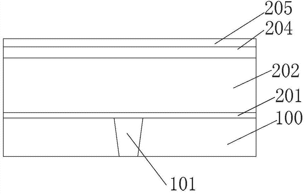
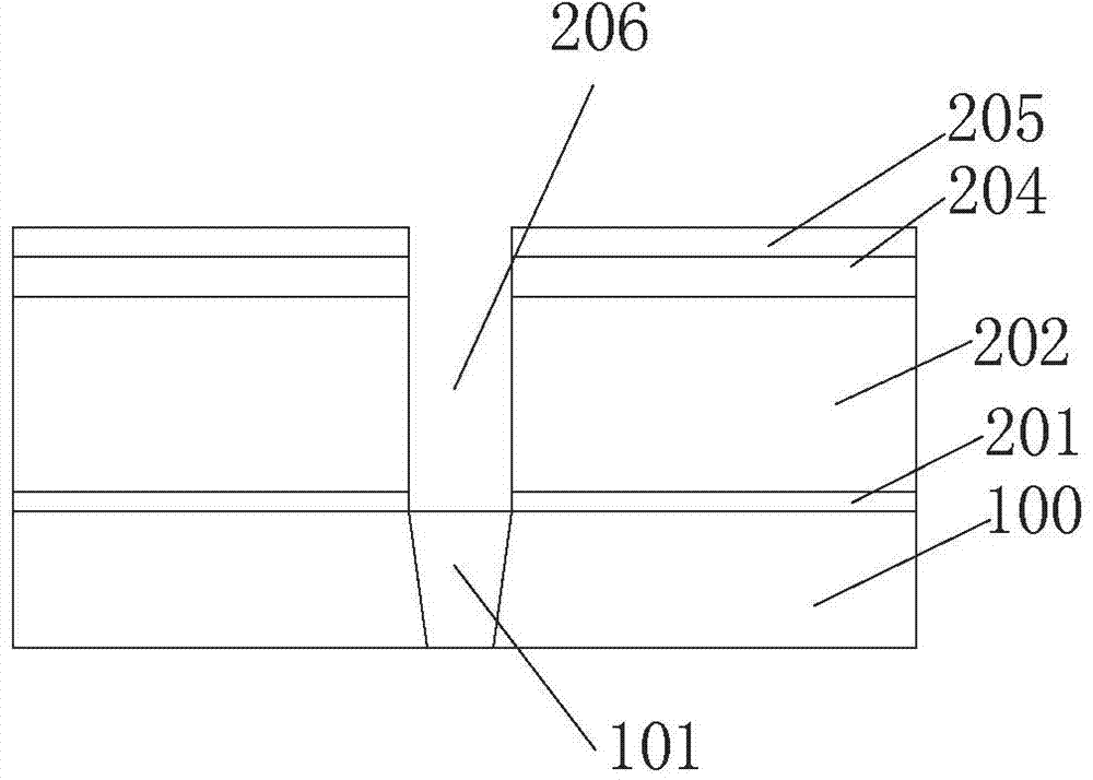
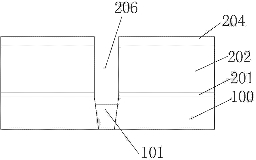
The invention provides a manufacture method for a first metal interconnection layer. The manufacture method includes the steps of: providing a semiconductor substrate; sequentially forming an etching stopping layer, an intermetallic dielectric layer, an ethyl orthosilicate oxide layer and a metal layer; etching the metal layer, the ethyl orthosilicate oxide layer, the intermetallic dielectric layer and the etching stopping layer to form a through hole; forming a sacrificial layer in the through hole; etching to remove the metal layer; stripping the sacrificial layer. The sacrificial layer is formed in the through hole, for preventing tungsten being corroded and damaged by etching liquid during the process of etching the metal layer, and thereby the defect that the tungsten is damaged in the prior art is overcome, and resistance between the first metal interconnection layer and a semiconductor device layer is reduced; after the metal layer is removed, the sacrificial layer is stripped, thus being free of additionally damaging the formed device structure.

Description

Technical field [0001] This application relates to the field of semiconductor manufacturing technology, and specifically to a method for manufacturing a first metal interconnection layer. Background technique [0002] In the manufacturing process of semiconductor devices, firstly perform semiconductor pre-processes to make various functional devices, and then make metal interconnection layers and other devices. Take metal oxide semiconductor field effect transistor (MOSFET) devices as an example. After the main structure of the device is completed, tungsten contacts and tungsten plugs are also made on the MOSFET device, and each part of the MOSFET device is electrically connected to each other to complete the device layer process of the MOSFET device. [0003] After the fabrication of the device layer where the MOSFET device is located, a metal interconnection layer must be fabricated on the device layer. In the manufacturing process of the metal interconnection layer in the prior...

Claims


Application Information

Patent Timeline
Patent Type & Authority Applications(China)
IPC IPC(8): H01L21/768
CPCH01L21/76877H01L21/76882
Inventor 刘焕新
Owner SEMICON MFG INT (SHANGHAI) CORP
Learn More