Radio-frequency LDMOS (Laterally Diffused Metal Oxide Semiconductor) device and technological method

A process method and device technology, applied in the field of radio frequency LDMOS devices, can solve the problem of high output capacitance of the device

Active Publication Date: 2015-07-01
SHANGHAI HUAHONG GRACE SEMICON MFG CORP
View PDF4 Cites 5 Cited by
  • Summary
  • Abstract
  • Description
  • Claims
  • Application Information

AI Technical Summary

Problems solved by technology

In general, in order to obtain higher carrier mobility, the P-type epitaxial layer ad

Method used


Image

  • Radio-frequency LDMOS (Laterally Diffused Metal Oxide Semiconductor) device and technological method
  • Radio-frequency LDMOS (Laterally Diffused Metal Oxide Semiconductor) device and technological method
  • Radio-frequency LDMOS (Laterally Diffused Metal Oxide Semiconductor) device and technological method

Examples


Embodiment Construction

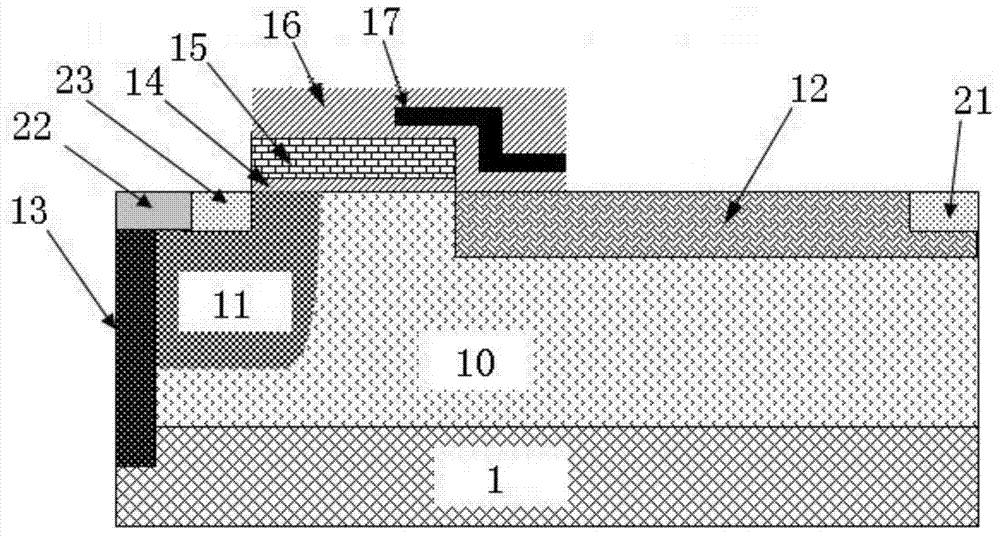
[0034] The radio frequency LDMOS device described in the present invention, such as Figure 9 As shown, there is a P-type epitaxy 10 on the P-type substrate 1, and the P-type epitaxy 10 has a P-type body region 11, and a heavily doped P-type region 22 located in the P-type body region 11 and the radio frequency the source region 23 of the LDMOS device;

[0035] The P-type epitaxy 10 also has a drift region of radio frequency LDMOS, and the drain region 21 of the LDMOS device is arranged in the drift region; the drift region is divided into a first drift region 121 of a lower layer and a second upper layer of different concentrations In the drift region 122 , the concentration of the first drift region 121 is higher than that of the second drift region 122 . And there are two-stage P-type buried layers 61 and 62 at the upper and lower junctions of the first drift region 121 and the second drift region 122 . The buried layer 61 is close to the edge of the gate terminal, locate...


PUM

PropertyMeasurementUnit
Thicknessaaaaaaaaaa

Abstract

The invention discloses a radio-frequency LDMOS (Laterally Diffused Metal Oxide Semiconductor) device. A body region and an N-type light-doped drift region are arranged in a P-type epitaxial layer on a P-type substrate; a polycrystalline silicon gate and a Faraday shield layer of the LDMOS device are arranged on the surface of the epitaxial layer; the N-type drift region is divided into an upper layer and a lower layer; the concentration of the lower layer is greater than that of the upper layer; two-section P-type buried layers are arranged at a junction of the upper layer and the lower layer; and the radio-frequency LDMOS device in the structure has lower output capacitance. The invention further discloses a technological method of the radio-frequency LDMOS device.

Description

technical field [0001] The invention relates to the field of semiconductors, in particular to a radio frequency LDMOS device, and the invention also relates to a process method of the radio frequency LDMOS device. Background technique [0002] RF LDMOS (LDMOS: Laterally Diffused Metal Oxide Semiconductor) device is a new generation of integrated solid-state microwave power semiconductor products formed by the integration of semiconductor integrated circuit technology and microwave electronic technology. It has good linearity, high gain, high withstand voltage, and output power. Large size, good thermal stability, high efficiency, good broadband matching performance, easy to integrate with MOS process, etc., and its price is much lower than that of gallium arsenide devices. It is a very competitive power device and is widely used in GSM , PCS, power amplifiers for W-CDMA base stations, as well as wireless broadcasting and nuclear magnetic resonance. [0003] In the design pr...

Claims


Application Information

Patent Timeline
IPC IPC(8): H01L29/78H01L29/06H01L21/336
Inventor 慈朋亮李娟娟钱文生刘冬华胡君段文婷石晶
Owner SHANGHAI HUAHONG GRACE SEMICON MFG CORP
Why Eureka
Try Eureka