A lateral high voltage device with multi-electrode structure

A lateral high voltage, multi-electrode technology, used in electrical components, semiconductor devices, circuits, etc., can solve the problem of increasing on-resistance of devices, and achieve the effects of reducing on-resistance, improving lateral withstand voltage, and increasing concentration

Active Publication Date: 2018-11-13
UNIV OF ELECTRONICS SCI & TECH OF CHINA
View PDF5 Cites 0 Cited by
  • Summary
  • Abstract
  • Description
  • Claims
  • Application Information

AI Technical Summary

Problems solved by technology

[0003] Aiming at the problem that the traditional lateral high-voltage power device adopts a drift region with a low doping concentration to increase the on-resistance of the device in order to obtain a high withstand voltage, the invention proposes a lateral high-voltage device with a multi-electrode structure

Method used


Image

  • A lateral high voltage device with multi-electrode structure
  • A lateral high voltage device with multi-electrode structure
  • A lateral high voltage device with multi-electrode structure

Examples


Embodiment 1

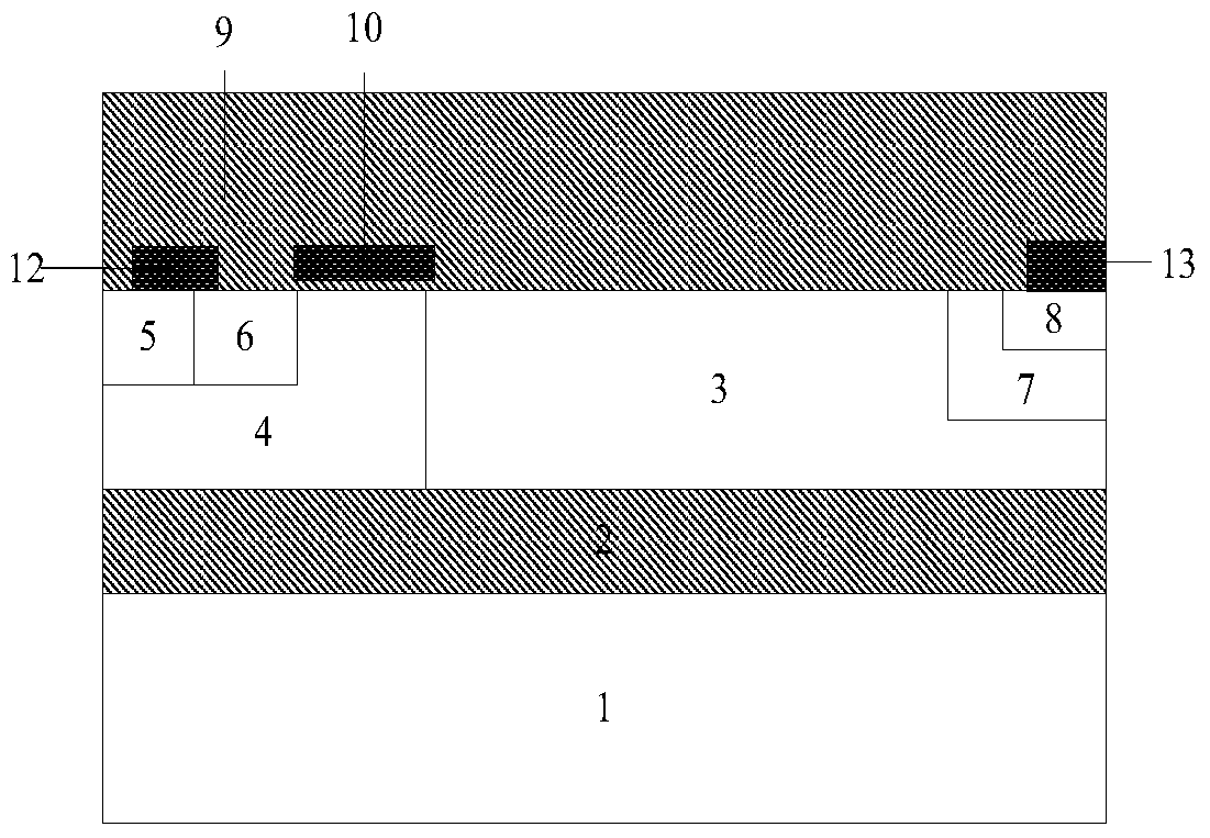
[0035] Such as figure 2As shown, a lateral high-voltage device with a multi-electrode structure includes a second-type impurity-doped semiconductor substrate 1; a buried oxide layer 2 formed on the second-type impurity-doped semiconductor substrate 1; formed on The first type doped impurity drift region 3 and the second type doped impurity well region 4 above the buried oxide layer 2; the second type doped impurity well region 4 formed in the second type doped impurity well region 4 The impurity contact region 5 and the first type doped impurity source region 6; the first type doped impurity well region 7 formed in the first type doped impurity drift region 3; the first type doped impurity well formed in the first type doped impurity well The first type doped impurity drain region 8 in the region 7; the dielectric layer 9 formed above the first type doped impurity drift region 3 and the second type doped impurity well region 4; in the dielectric layer 9 A polysilicon gate 10...

Embodiment 2

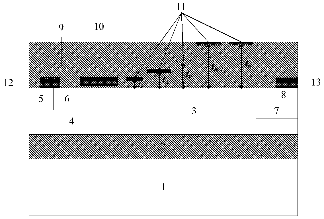
[0037] Such as image 3 As shown, the difference between the present embodiment and embodiment 1 is: the number of the electrodes is n, the height of the electrodes (that is, the distance between the lower surface of the electrode and the upper surface of the first type doped impurity drift region 3 ) has a rising trend along the direction from the second-type doped impurity well region 4 to the first-type doped impurity well region 7, and the electrodes 11 are always biased at different potentials and are farther away from the first-type doped impurity well region 7 Closer, the closer the potential of the electrode bias is to the potential on the drain region 8 of the first type doped impurity when the device breaks down.

Embodiment 3

[0039] Such as Figure 4 As shown, the difference between this embodiment and embodiment 2 is that the SOI structure is replaced by a bulk silicon structure, that is, the buried oxide layer 2 is removed. It is illustrated that the present invention can be used for both SOI devices and bulk silicon devices.


PUM


Abstract

The invention provides a lateral high-voltage device with a multi-electrode structure, which belongs to the field of semiconductor power devices. Including second-type doped impurity semiconductor substrate, first-type doped impurity drift region, second-type doped impurity well region, second-type doped impurity contact region, first-type doped impurity source region, first-type impurity doped impurity well region, first type doped impurity drain region, dielectric layer, polysilicon gate, source metal and drain metal; In the dielectric layer above the region between the impurity well regions, there are also n electrodes, n≥2, there is an interval between the projections of any two electrodes in the lateral direction in the n electrodes, and each electrode is biased at different potentials. The lateral high-voltage device provided by the present invention can reduce the on-resistance of the device while increasing the withstand voltage of the device, thereby effectively alleviating the contradiction between the on-resistance and the withstand voltage of the lateral high-voltage device.

Description

technical field [0001] The invention belongs to the field of semiconductor power devices, in particular to a lateral high-voltage device with a multi-electrode structure. Background technique [0002] Lateral high-voltage devices are an essential part of the development of high-voltage power integrated circuits. They have the advantages of high withstand voltage, high input impedance, good safe working area, and low power consumption. They have been widely used in motor drives, automotive electronics, and industrial control. in the power switching device. When the lateral high-voltage device works in a high withstand voltage environment, it needs to adopt a long drift region, so the lateral high-voltage device will be accompanied by high on-resistance, resulting in higher power consumption of the device during normal operation. In practical applications, it is necessary to reduce the on-resistance of the device as much as possible while ensuring the withstand voltage of the...

Claims


Application Information

Patent Timeline
Patent Type & Authority Patents(China)
IPC IPC(8): H01L29/78H01L29/06
CPCH01L29/0607H01L29/7393H01L29/7816
Inventor 乔明周锌李阳代刚陈钢张波
Owner UNIV OF ELECTRONICS SCI & TECH OF CHINA
Why Eureka
Try Eureka