Decorative-material-attached substrate and manufacturing method therefor, touch panel and information display device

A decorative material and a manufacturing method technology, which are applied in identification devices, input/output processes of data processing, instruments, etc., can solve problems such as difficulty in improving optical density, and achieve the effect of small b value

Active Publication Date: 2015-07-01
FUJIFILM CORP
View PDF33 Cites 2 Cited by
  • Summary
  • Abstract
  • Description
  • Claims
  • Application Information

AI Technical Summary

Problems solved by technology

[0005] On the other hand, when using a white coloring layer as a decorative material, there is a problem that it is difficult to increase its optical density

Method used


Image

  • Decorative-material-attached substrate and manufacturing method therefor, touch panel and information display device
  • Decorative-material-attached substrate and manufacturing method therefor, touch panel and information display device
  • Decorative-material-attached substrate and manufacturing method therefor, touch panel and information display device

Examples


Embodiment 1~ Embodiment 3 and comparative example 1

[0267]

[0268] Black coloring liquid 1 - black coloring liquid 4, white coloring liquid 1, and white coloring liquid 2 described in Table 1 below were prepared using the following materials.

[0269] [Table 1]

[0270]

[0271]

[0272] ・Black dispersion liquid 1 (GB4016, manufactured by Sanyo Pigment Co., Ltd., the following composition)

[0273] Black pigment (carbon black) 25.0% by mass

[0274] Dispersion aid 9.5% by mass

[0275] Dispersion solvent (propylene glycol monomethyl ether acetate) 65.5% by mass

[0276] · Black dispersion liquid 2 (CDP-K106, manufactured by FUJIFILM Electronic Materials Co., Ltd., the following composition)

[0277] Black pigment (titanium dioxide) 25.0% by mass

[0278] Dispersion aid 7.0% by mass

[0279] Dispersion solvent (methyl ethyl ketone) 68.0% by mass

[0280] ・White dispersion (FP White (FP White) B422, manufactured by Sanyo Pigment Co., Ltd., with the following composition)

[0281] White pigment (titanium dioxide) 7...

Embodiment 101

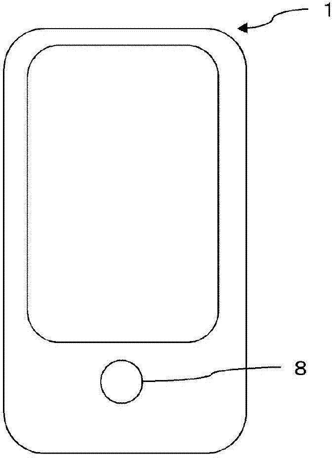
[0363] [Example 101: Production of touch screen]

[0364] "Formation of the first transparent electrode pattern"

[0365]

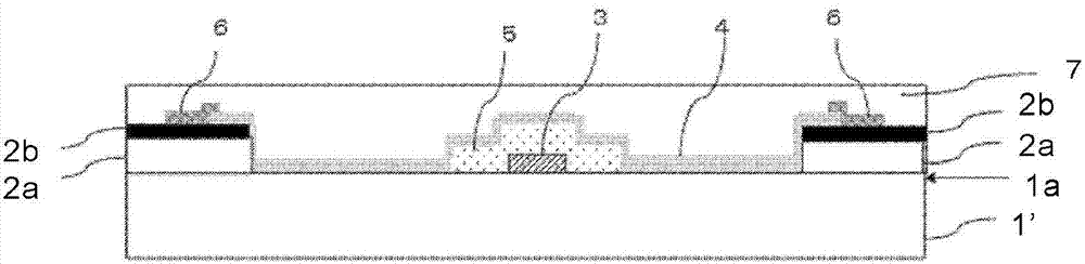
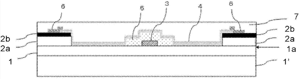
[0366] The base material with decoration material of each embodiment is introduced into the vacuum chamber, using SnO 2 The ITO target (target) (indium: tin=95:5 (molar ratio)) with a content rate of 10% by mass was subjected to direct current (Direct Current, DC) magnetron sputtering (condition: the temperature of the base material was 250° C. , the argon gas pressure is 0.13Pa, and the oxygen pressure is 0.01Pa) to form an ITO thin film with a thickness of 40nm to obtain a front panel with a transparent electrode layer formed thereon. The surface resistance of the ITO thin film was 80Ω / □.

[0367]

[0368] In the preparation of the white transfer material 1 of the above-mentioned production example 1, the above-mentioned white coloring liquid 1 was replaced with the coating liquid for the photocurable resin layer for etching containing the followi...

Embodiment 106

[0441] The front panel of Example 106 was obtained by performing the same operations as in Example 101, except that the base material with a decorative material of Example 6 was used instead of the base material with a decorative material of Example 1. This front panel is also preferable as the front panels of other embodiments.


PUM

PropertyMeasurementUnit
thicknessaaaaaaaaaa
thicknessaaaaaaaaaa
thicknessaaaaaaaaaa

Abstract

The present invention provides a decorative-material-attached substrate having a white colored layer and a light blocking layer, and for which the b value of the white colored layer after high temperature processing is small. This decorative-material-attached substrate has in the following order a substrate, the white colored layer, and the light blocking layer. Both the white colored layer and the light blocking layer include a resin having a siloxane bond in the main chain.

Description

technical field [0001] The present invention relates to a base material with a decorative material, a manufacturing method thereof, a touch panel provided with the base material provided with the decorative material, and an information display device provided with the touch panel. Background technique [0002] In electronic equipment such as mobile phones, car navigation (car navigation), personal computers (personal computers), ticket vending machines, and bank terminals, touch-screen input devices have been arranged on the surfaces of liquid crystal devices in recent years. Information corresponding to the pointing image is input by bringing a finger or a touch pen (touch pen) into contact with the point where the pointing image is displayed in the image display area of ​​the display area. [0003] Such an input device (touch panel) includes a resistive film type, a capacitive type, and the like. Capacitive input devices have an advantage that only a light-transmitting co...

Claims


Application Information

Patent Timeline
Patent Type & Authority Applications(China)
IPC IPC(8): G06F3/041G02F1/1333G06F3/044G09F9/00
CPCG06F3/044G06F3/0443G06F3/0446
Inventor 并河均有冨隆志后藤英范
Owner FUJIFILM CORP
Why Eureka
Try Eureka