led testing process and correction method for this

A technology of testing process and correction function, which is applied in the direction of photometry, semiconductor/solid-state device testing/measurement, measuring device, etc., and can solve problems that are not suitable for high-capacity testing applications

Active Publication Date: 2017-08-25
ASM TECH SINGAPORE PTE LTD
View PDF4 Cites 0 Cited by
  • Summary
  • Abstract
  • Description
  • Claims
  • Application Information

AI Technical Summary

Problems solved by technology

The problem with this approach is that in addition to the direct detection of light emitted by the device under test (DUT: device under test), the integrated ball used as part of the test procedure can detect indirect light from inactive LEDs adjacent to the DUT. the light
However, this equipment is generally not suitable for high-throughput testing applications because it requires precise manual positioning in the horizontal and vertical directions for the tapered adapter to be effective.

Method used


Image

  • led testing process and correction method for this
  • led testing process and correction method for this
  • led testing process and correction method for this

Examples


Embodiment Construction

[0044] Embodiments of the present invention provide a method for directly testing an array of LED units on a substrate without first requiring dicing. Profiles of test results containing measured optical and electrical properties as a function of position in the array can be generated and used to bin LEDs prior to dicing and packaging. This method has a higher throughput than previously known methods because less cell sorting processing is required. The risk of damage or contamination is also reduced due to the reduced overall sorting volume.

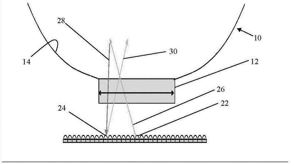
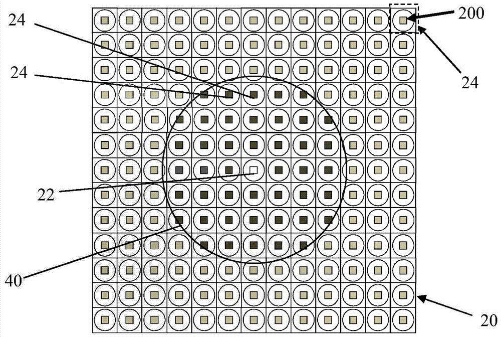
[0045]The inventors of the present invention have realized for the first time that LEDs can be tested in-panel at high throughput by substantially modifying the light re-emitted from the phosphors of those LEDs that are not activated adjacent to the DUT. The re-lit puzzle set forth in figure 1 , wherein a detector device comprising an integrated ball 10 with an input port 12 is placed above the LED 22 (DUT), which is activated and emi...


PUM


Abstract

The invention discloses a method for generating a correction function for an LED testing process, the method comprising the following steps: within the field of view of a detector, detecting light emitted by a reference LED and from one or more LEDs located on a board light reflected by inactive LEDs; the number of said inactive LEDs in the field of view is varied such that an erroneous value for at least one optical parameter is obtained as a function of the number of inactive LEDs in the field of view; detected in the absence of any other LEDs to determine at least one reference value of the or each said optical parameter by reference to light emitted by an active LED or by an active LED, the active LED and the reference LED having the same optical properties; and calculating the error value and the or each reference The difference between the values ​​to generate a correction function that is dependent on the number of inactive LEDs disposed within the detector's field of view when the detector detects light emitted by the LED under test conditions.

Description

technical field [0001] The present invention relates to a method and device for generating a correction factor distribution map (map) for an LED testing process, and to an LED testing process. Background technique [0002] The LED manufacturing process generally includes an arrayed LED unit structure on a PCB (printed circuit board) substrate. The construction method includes die mount, wire bonding, phosphor application, and lens mount, followed by singulation to cut the PCB into individual LED units. Segmented LED units are individually tested and sorted into bins based on optical and electrical properties prior to packaging. [0003] Optical testing of LED units is typically accomplished by placing the LED inside the input port of an integrating sphere coupled to a detector (eg via fiber optics to a spectrometer), measuring the optical parameters of the LED unit, And the LED unit is calibrated by comparing the measured optical parameters with respect to the optical para...

Claims


Application Information

Patent Timeline
Patent Type & Authority Patents(China)
IPC IPC(8): H01L33/00H01L21/66
CPCG01J1/42G01J1/0437G01J2001/0481G01J2001/4252G01N21/274G01N2201/0622G01N2201/0623G09G2320/045
Inventor 麦家仪汪世杰刘晓兰俱剑君
Owner ASM TECH SINGAPORE PTE LTD
Why Eureka
Try Eureka