Structure of broadband wave absorber and preparation method

A wave absorber and broadband technology, applied in the field of integrated optics, can solve the problems of narrow absorption angle, weakened absorption, and limited application of wave absorbers.

Inactive Publication Date: 2015-07-15
HARBIN INST OF TECH SHENZHEN GRADUATE SCHOOL
View PDF2 Cites 13 Cited by
  • Summary
  • Abstract
  • Description
  • Claims
  • Application Information

AI Technical Summary

Problems solved by technology

The frequency of the electromagnetic waves absorbed by the general multi-frequency absorber is scattered, it cannot achieve continuous absorption, and the absorption of several frequencies will compromise with each other, and it cannot be taken into account, resulting in weakened absorption.
Broadband absorbers generally adopt a multi-layer design, and

Method used


Image

  • Structure of broadband wave absorber and preparation method
  • Structure of broadband wave absorber and preparation method
  • Structure of broadband wave absorber and preparation method

Examples


Embodiment Construction

[0031] The present invention will be further described below in conjunction with the drawings.

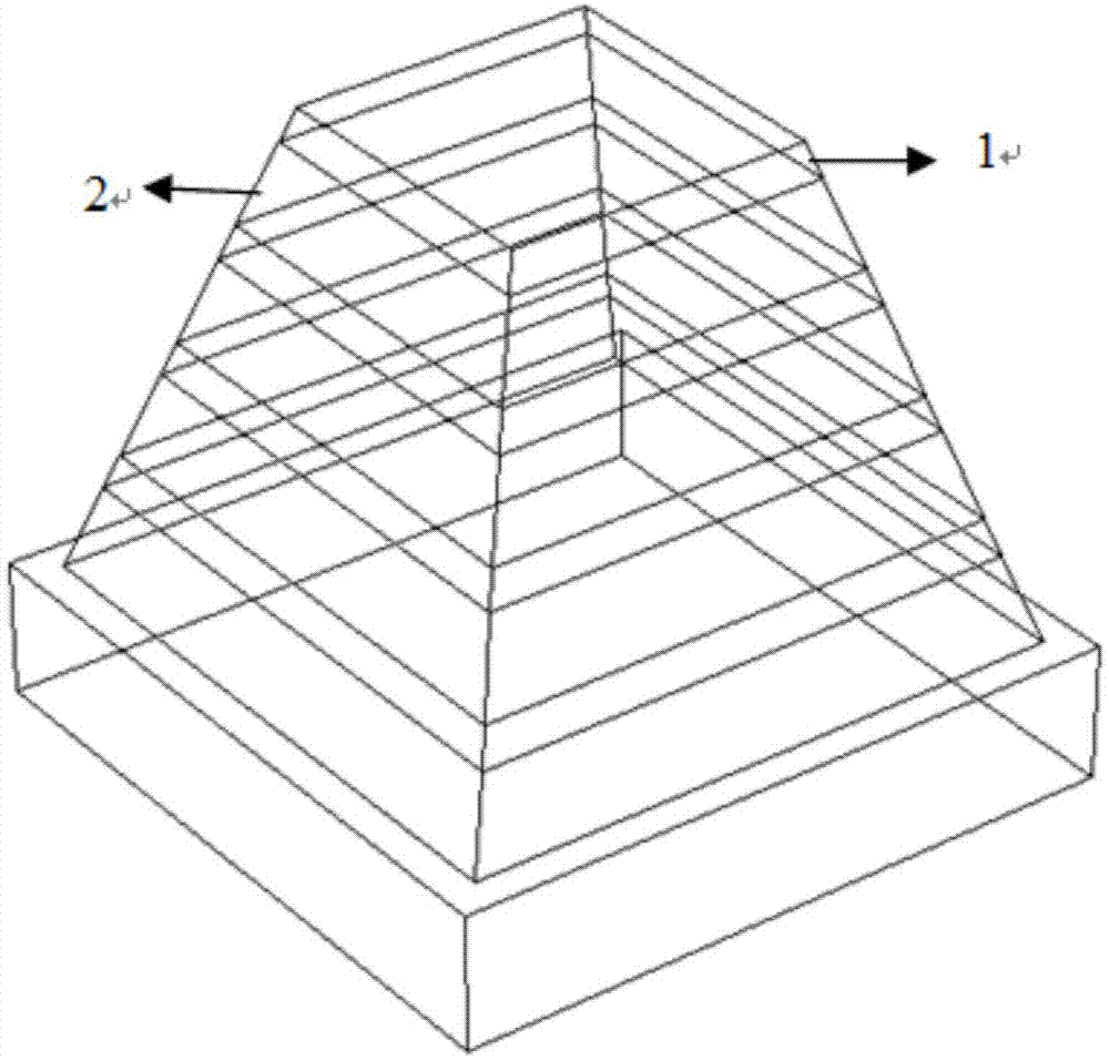
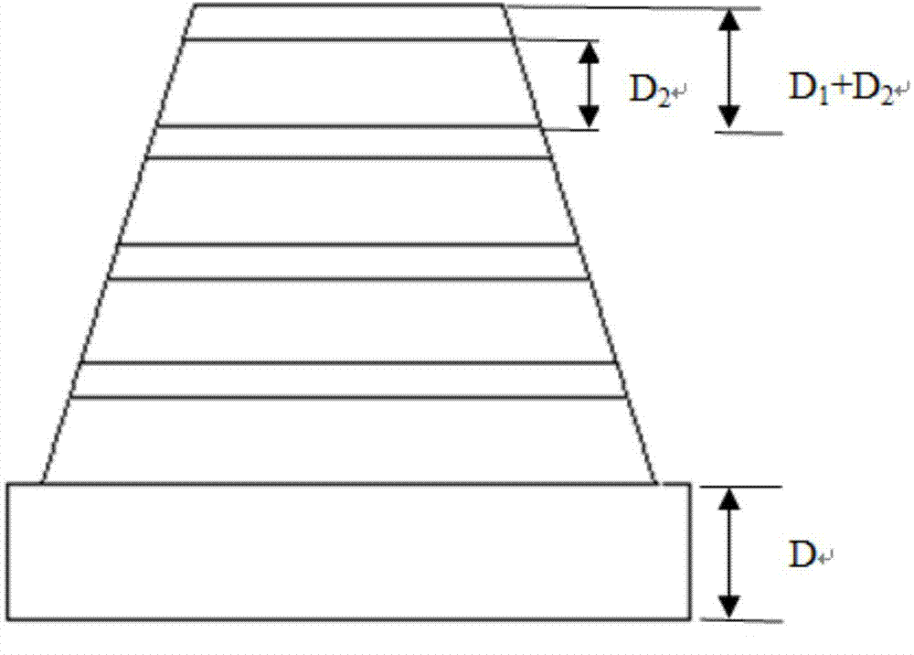
[0032] In this design, the absorber adopts a semi-pyramid structure. The pyramid is composed of multiple layers of metal-dielectric layers alternately superimposed. When electromagnetic waves are incident on the absorber, due to the effect of localized surface plasmon resonance at the metal-medium interface, opposite electric charges are accumulated in the metal layer of the absorber, which excites electric dipoles in the metal film. Resonance leads to an increase in the local electric field. Due to the coupling effect of the electric dipole, a magnetic dipole is generated in the adjacent metal layer, and the effect of the magnetic dipole in turn leads to the enhancement of the magnetic field in the dielectric layer. Since the metal and dielectric layers have different widths, different widths correspond to different response frequencies. When the width is wider, the corresponding ...


PUM

PropertyMeasurementUnit
Media thicknessaaaaaaaaaa
Thicknessaaaaaaaaaa
Media thicknessaaaaaaaaaa

Abstract

The invention provides a structure of a broadband wave absorber and a preparation method. The structure comprises a substrate layer and a half-pyramid structure arranged on the substrate layer, wherein the half-pyramid structure is formed by alternately stacking and combining multiple metal-medium layers, the size of the structure is decreased progressively from bottom to top in the Z direction, the structure is a symmetrical structure, and the axis of symmetrical is a connecting line of centers of the metal-medium layers. A substrate is coated with the metal-medium layers sequentially with a coating method, and then the half-pyramid structure is etched. The structure is simple: the structure of the wave absorber is single and convenient to prepare. The spectrum is easy to measure: at the measurement stage, the band ranging from 8 mu m to 14 mu m is a middle infrared band, and the transmission and reflection spectrum of the structure can be acquired easily by the aid of existing equipment, so that the absorption spectrum is acquired.

Description

Technical field [0001] The invention relates to the field of integrated optics, in particular to the structure and preparation method of a broadband wave absorber. Background technique [0002] For electromagnetic waves of a specific frequency, the absorption bandwidth of the existing wave absorber is narrow and cannot achieve high absorption in the entire spectrum. [0003] For electromagnetic waves of a specific frequency, the absorption angle of the existing wave absorber is small, and it cannot achieve high absorption in a large angle range. [0004] For electromagnetic waves of specific frequencies, existing wave absorbers are sensitive to the polarization direction of the incident electromagnetic waves, and cannot achieve good absorption. [0005] According to the absorption bandwidth, the existing wave absorbers can be divided into three types: narrowband absorbers, multi-frequency absorbers and broadband absorbers. Its structure generally adopts a metal-dielectric-metal three...

Claims


Application Information

Patent Timeline
IPC IPC(8): H01Q17/00
Inventor 肖淑敏刘佳宋清海
Owner HARBIN INST OF TECH SHENZHEN GRADUATE SCHOOL
Why Eureka
Try Eureka