Ceramic circuit board, semiconductor device, and method for manufacturing ceramic circuit board

A technology for wiring substrates and ceramics, used in semiconductor devices, semiconductor/solid-state device parts, manufacturing tools, etc., can solve the problems of uneven shrinkage, high sintering temperature, and cannot eliminate the lowering of the position accuracy of upper and lower via holes, and achieve high The effect of reliability

Inactive Publication Date: 2015-07-15
ALLIED MATERIAL
View PDF8 Cites 7 Cited by
  • Summary
  • Abstract
  • Description
  • Claims
  • Application Information

AI Technical Summary

Problems solved by technology

However, in this method, the sintering temperature is higher, reaching 1500°C or higher. In practice, Al and Si constituting the substrate during sintering diffuse to the upper and lower conductors during sintering, so the generation of voids cannot be avoided.
In addition, since the upper and lower via holes are formed in advance and then sintered in the ceramic green sheet which is the base material of the substrate, the upper and lower via holes cannot be eliminated due to uneven shrinkage during sintering of the ceramic green sheet. The problem of reduced position accuracy

Method used


Image

  • Ceramic circuit board, semiconductor device, and method for manufacturing ceramic circuit board
  • Ceramic circuit board, semiconductor device, and method for manufacturing ceramic circuit board
  • Ceramic circuit board, semiconductor device, and method for manufacturing ceramic circuit board

Examples


Embodiment 1

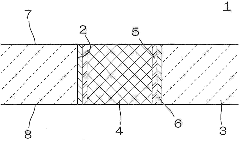
[0199] (Formation of upper and lower via holes 2)

[0200] On an AlN substrate 3 of □100×t0.5 mm polished to a surface roughness Ra of 0.5 μm, 3000 vertical via holes 2 of φ0.5 mm were formed using a YAG laser. The positional accuracy of the formed upper and lower via holes 2 was measured using a tool microscope and found to be ±20 μm.

[0201] (Formation of Adhesive Layer 6 and Intermediate Layer 5)

[0202] The substrate 3 formed with the upper and lower via holes 2 was ultrasonically cleaned with isopropyl alcohol (IPA), and the IPA was volatilized by air blowing, and then dried by heating in an oven at 100° C. for 10 minutes.

[0203] Then, on the surfaces 7 and 8 on both sides of the substrate 3 and the inner surfaces of the upper and lower via holes 2, a Ti film with a thickness of 0.1 μm as the adhesive layer 6 and a Ti film with a thickness of 1.0 μm as the intermediate layer 5 were sequentially formed by sputtering. The W film.

[0204] The film is formed in the sp...

Embodiment 2

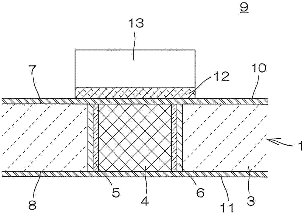
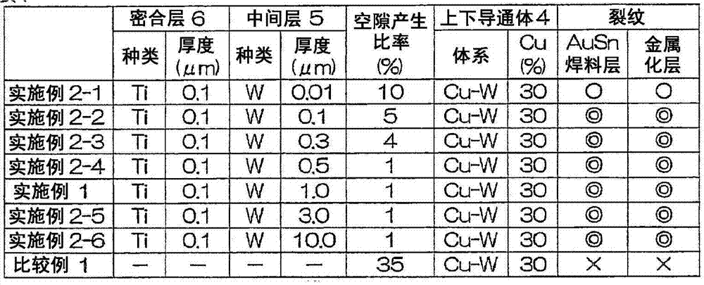
[0241] Except that the thickness of the W film as the intermediate layer 5 is set to 0.01 μm (Example 2-1), 0.1 μm (Example 2-2), 0.3 μm (Example 2-3), 0.5 μm (Example 2- 4), 3.0 μm (Example 2-5), and 10.0 μm (Example 2-6), complete the ceramic wiring substrate 1 in the same manner as Example 1, form metallization layers 10, 11, and the metallization The cross-sectional observations 1 and 2 were performed after the layers 10 and 11 were patterned. The results are shown in Table 1 together with the results of Example 1 and Comparative Example 1.

[0242] [Table 1]

[0243] Table 1

[0244]

[0245] According to the results of Example 1, Examples 2-1 to 2-6, and Comparative Example 1 in Table 1, it is known that by forming a W film as an intermediate layer 5 on the inner surface of the upper and lower via holes 2, the W film from the ceramics can be suppressed. Diffusion of Al in the substrate 3 made and the generation ratio of voids in the upper and lower conductors 4 cau...

Embodiment 3

[0248] In addition to being the intermediate layer 5, forming a thickness of 0.01 μm (Example 3-1), 0.1 μm (Example 3-2), 0.3 μm (Example 3-3), 0.5 μm (Example 3-4), 1.0 μm (Example 3-5), 3.0 μm (Example 3-6), or 10.0 μm (Example 3-7) Mo film, complete the ceramic wiring substrate 1 in the same manner as in Example 1, and form a metallization layer 10. , 11, and after patterning the metallized layers 10, 11, cross-sectional observations 1, 2 were implemented. The results are shown in Table 2 together with the results of Comparative Example 1.

[0249] [Table 2]

[0250] Table 2

[0251]

[0252] From the results of Examples 3-1 to 3-7 and Comparative Example 1 in Table 2, it is known that the same effect as that of the W film of Examples 1 and 2 can be obtained even when a Mo film is formed as the intermediate layer 5 .

[0253] That is, it was found that by forming a Mo film as the intermediate layer 5 on the inner surface of the upper and lower via holes 2, the diffus...


PUM

PropertyMeasurementUnit
thicknessaaaaaaaaaa
thicknessaaaaaaaaaa
thicknessaaaaaaaaaa

Abstract

Provided is a ceramic wiring substrate comprising a vertical conducting body which is formed by forming a vertical conducting hole in a substrate after the substrate is formed in a plate shape by sintering a ceramic precursor, forming a porous structure made of a metal with a high melting point in the vertical conducting hole, and infiltrating a low-resistance metal into the hole. The vertical conducting body has a normal composite structure with no abnormal grain growth, voids, cracks, or the like, and has no possibility of sloughing from the substrate. Also provided are a method for manufacturing the ceramic wiring substrate, and a semiconductor device configured using the ceramic wiring substrate. On the inner surface of the vertical conducting hole (2) of the substrate (3) before the vertical conducting body (4) having the composite structure is formed, an intermediate layer (5) comprising at least one from among the group consisting of Mo, W, Co, Fe, Zr, Re, Os, Ta, Nb, Ir, Ru, and Hf is formed.

Description

technical field [0001] The present invention relates to a ceramic wiring board including a plate-shaped substrate made of ceramics containing at least Al or Si, upper and lower conductors penetrating the substrate in a thickness direction, and a semiconductor device using the ceramic wiring board. Background technique [0002] In materials such as AlN, Al 2 o 3 , SiC, and other ceramics formed in a plate shape, vertical via holes penetrating in the thickness direction are formed at predetermined positions on the substrate, and ceramic wiring substrates filled with vertical vias (via holes) are used for mounting semiconductor elements. [0003] For this ceramic wiring board, in order to improve the positional accuracy of the upper and lower via holes, it is generally practiced to firstly sinter the board body (ceramic green sheet) which is the precursor of the ceramic base material to form the board, After forming the upper and lower via holes penetrating through the thickn...

Claims


Application Information

Patent Timeline
Patent Type & Authority Applications(China)
IPC IPC(8): H01L23/13B22F3/26B22F7/06C22C5/02C22C5/06C22C9/00C22C27/04H05K1/09H05K3/40
CPCC22C27/04H01L2924/0002H05K1/092C22C9/00C22C5/06H01L23/3677C22C5/02B22F2998/10H05K3/4061H01L23/15H05K1/0204H05K1/0306Y10T29/49126C22C14/00B32B15/00B23K35/0233B23K35/262C22C5/04H01L2924/00B22F7/004B22F3/26H05K1/115H05K1/18
Inventor 广濑义幸杉谷幸爱胡间纪人丰岛刚平上西升
Owner ALLIED MATERIAL
Why Eureka
Try Eureka