Single-silicon-wafer compound sensor structure with pressure sensor embedded in accelerometer and manufacturing method

A technology of acceleration sensor and pressure sensor, which is applied in acceleration measurement using inertial force, fluid pressure measurement by changing ohmic resistance, measurement of property force using piezoelectric resistance material, etc. It can improve the detection accuracy, reduce the chip size, and reduce the production cost.

Active Publication Date: 2015-07-22
SHANGHAI INST OF MICROSYSTEM & INFORMATION TECH CHINESE ACAD OF SCI
View PDF13 Cites 8 Cited by
  • Summary
  • Abstract
  • Description
  • Claims
  • Application Information

AI Technical Summary

Problems solved by technology

[0006] The main technical problem to be solved by the present invention is to provide a single-silicon chip composite sensor structure and method with an accelerometer embedded pressure sensor, so as to solve the problems of traditional composite sensor chip structure size, high cost, and complicated manufacturing process.

Method used


Image

  • Single-silicon-wafer compound sensor structure with pressure sensor embedded in accelerometer and manufacturing method
  • Single-silicon-wafer compound sensor structure with pressure sensor embedded in accelerometer and manufacturing method
  • Single-silicon-wafer compound sensor structure with pressure sensor embedded in accelerometer and manufacturing method

Examples


Embodiment Construction

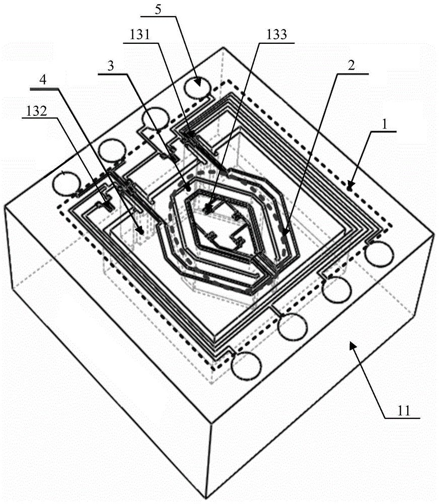
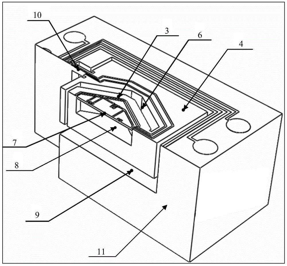
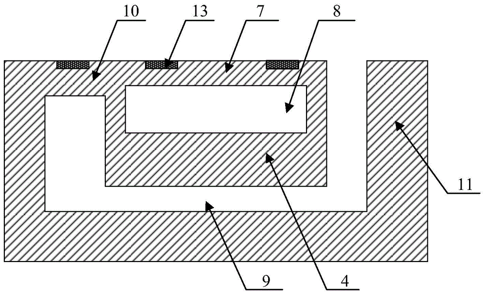
[0070] Embodiments of the present invention are described below through specific examples, and those skilled in the art can easily understand other advantages and effects of the present invention from the content disclosed in this specification. The present invention can also be implemented or applied through other different specific implementation modes, and various modifications or changes can be made to the details in this specification based on different viewpoints and applications without departing from the spirit of the present invention.

[0071] see figure see Figure 1 to Figure 10 . It should be noted that the diagrams provided in this embodiment are only schematically illustrating the basic concept of the present invention, although only the components related to the present invention are shown in the diagrams rather than the number, shape and Dimensional drawing, the type, quantity and proportion of each component can be changed arbitrarily during actual implement...


PUM

PropertyMeasurementUnit
lengthaaaaaaaaaa
widthaaaaaaaaaa
thicknessaaaaaaaaaa

Abstract

The invention relates to a single-silicon-wafer compound sensor structure with a pressure sensor embedded in an accelerometer and a manufacturing method. The compound sensor structure comprises a single silicon wafer, and an accelerated speed sensor and a pressure sensor which are integrated on the single silicon wafer, wherein the accelerated speed sensor and the pressure sensor are integrated on the surface of the single silicon wafer; the pressure sensor is suspended at the central position of a mass block of the accelerated speed sensor; a pressure reference cavity is directly buried into the mass block. According to the single-silicon-wafer compound sensor structure, the size of a chip is greatly reduced by the accelerated speed sensor and the pressure compound sensor, and the manufacturing cost is reduced; the structure is combined with an IC process so that large-batch manufacturing can be realized; meanwhile, the pressure sensor is directly suspended at the central position of the mass block, namely the size of the chip can be reduced to the greatest extent, and the mutual crosstalk of a detection signal between the accelerated speed sensor and the pressure sensor is also effectively eliminated, so that the detection precision of the compound sensor is greatly improved.

Description

technical field [0001] The invention belongs to the technical field of silicon micromechanical sensors, and relates to a single silicon chip composite sensor structure and method with an accelerometer embedded with a pressure sensor. Background technique [0002] With the continuous advancement of MEMS technology, MEMS composite sensors have been widely used in various industries due to their advantages such as smaller chip structure size, lower manufacturing cost, superior performance and lower subsequent installation and application costs, such as: automotive electronics , aerospace, consumer electronics, biomedicine, and more. For this reason, a large number of scientific researchers and major MEMS product development companies have invested a lot of scientific research capacity to develop different types of composite sensor chips to meet the growing market demand. At present, the most notable applications of composite sensors are ten-axis Combos composite sensor chips i...

Claims


Application Information

Patent Timeline
Patent Type & Authority Applications(China)
IPC IPC(8): G01P15/12G01L1/18G01L9/06
Inventor 王家畴李昕欣
Owner SHANGHAI INST OF MICROSYSTEM & INFORMATION TECH CHINESE ACAD OF SCI
Why Eureka
Try Eureka