Semiconductor device and manufacturing method thereof

A manufacturing method and semiconductor technology, applied in the direction of semiconductor/solid-state device manufacturing, semiconductor devices, radiation control devices, etc., can solve problems such as pollution, increased manufacturing costs, and difficulty in improving yields, and achieve cost reduction, manufacturing cost reduction, and good quality. rate-boosting effect

Active Publication Date: 2015-07-22
XINTEC INC
View PDF6 Cites 7 Cited by
  • Summary
  • Abstract
  • Description
  • Claims
  • Application Information

AI Technical Summary

Problems solved by technology

[0004] However, after the glass sheet is removed from the wafer, the subsequent process is still continued at the wafer level, so the image sensing area of ​​the wafer is easily contaminated during the process, making it difficult to improve the yield
In order to avoid product contamination, the process after the glass sheet is removed from the wafer needs to be performed in a clean room, thus increasing the cost of clean room equipment and technicians
In addition, the high price of ultraviolet light tape will also cause an increase in manufacturing costs

Method used


Image

  • Semiconductor device and manufacturing method thereof
  • Semiconductor device and manufacturing method thereof
  • Semiconductor device and manufacturing method thereof

Examples


Embodiment Construction

[0060] A number of embodiments of the present invention will be disclosed in the following figures. For the sake of clarity, many practical details will be described together in the following description. It should be understood, however, that these practical details should not be used to limit the invention. That is, in some embodiments of the present invention, these practical details are unnecessary. In addition, for the sake of simplifying the drawings, some conventional structures and elements will be shown in a simple and schematic manner in the drawings.

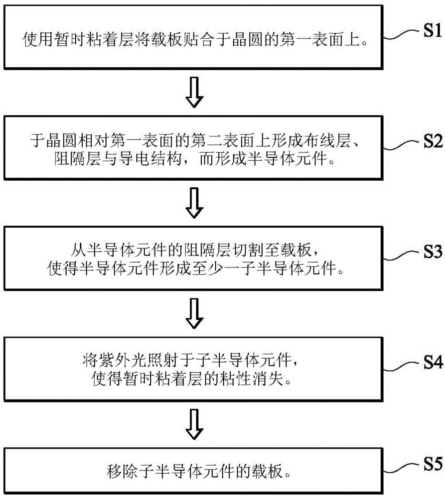
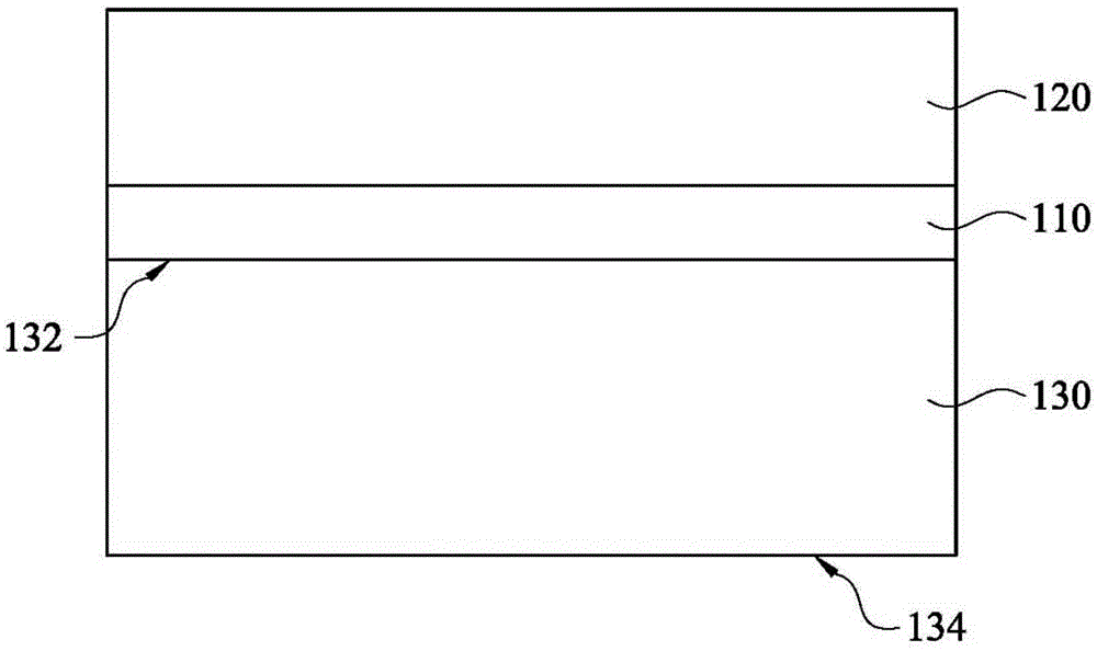
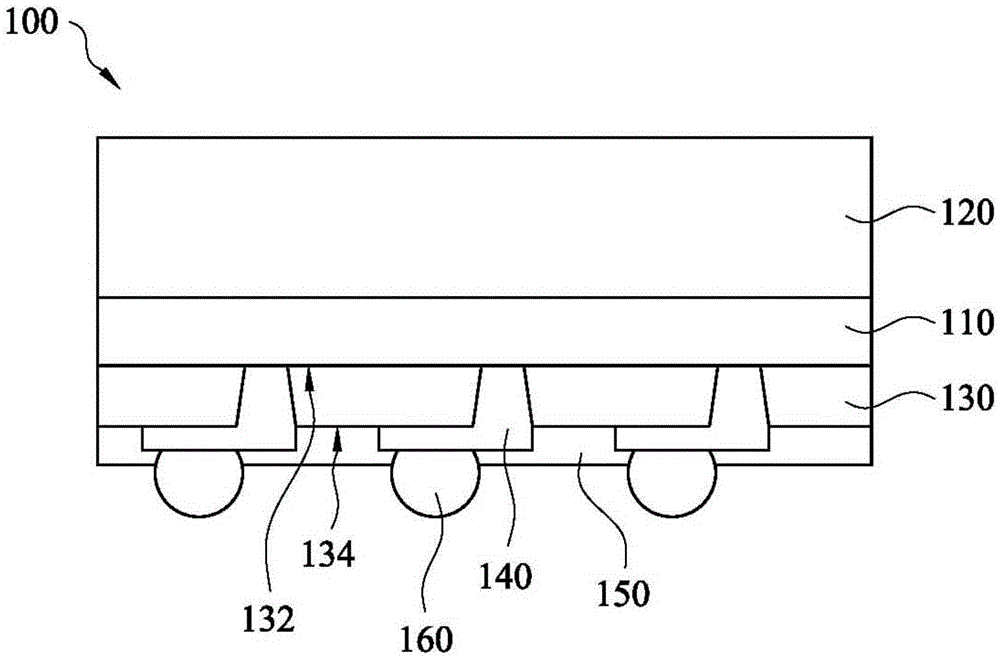
[0061] figure 1 A flowchart illustrating a method for manufacturing a semiconductor device according to an embodiment of the present invention. The manufacturing method of the semiconductor device includes the following steps: firstly, in step S1, the carrier board is pasted on the first surface of the wafer by using a temporary adhesive layer. Next, in step S2, a wiring layer, a barrier layer and a conductive stru...


PUM


Abstract

A manufacturing method of a semiconductor device includes the following steps. A temporary bonding layer is used to adhere a carrier to a first surface of a wafer. A redistribution layer, an insulating layer, and a conductive structure are formed on a second surface of the wafer opposite to the first surface, such that a semiconductor element is formed. The semiconductor element is diced from the insulating layer to the carrier, such that the semiconductor element forms at least one sub-semiconductor element. UV light is used to irradiate the sub-semiconductor element, such that adhesion of the temporary bonding layer is eliminated. The carrier of the sub-semiconductor element is removed.

Description

technical field [0001] The present invention relates to a semiconductor device and a manufacturing method of the semiconductor device. Background technique [0002] When manufacturing image sensor wafers (such as CMOS), glass sheets are usually covered on the surface of the wafer to protect the wafer and prevent dust from adhering to the image sensing area of ​​the wafer. However, when the wafers formed after dicing are used in electronic products, the electronic products usually have a light-transmitting sheet on the housing that aligns the wafers, and the light-transmitting sheet has a similar protective function to the glass sheet on the surface of the wafer. When there is no glass sheet on the surface of the wafer, although the light transmittance can be improved and the image sensing ability of the wafer after dicing is improved, but because the thickness of the wafer is very thin, it is necessary to move the wafer on which the ball grid array has been formed. is quite...

Claims


Application Information

Patent Timeline
Patent Type & Authority Applications(China)
IPC IPC(8): H01L21/301H01L21/78H01L27/146
CPCH01L27/14632H01L27/1469H01L27/1463H01L27/14634H01L27/14687H01L27/14685H01L31/0203H01L27/14636H01L27/14627H01L27/14618H01L2224/11
Inventor 李柏汉张恕铭刘沧宇何彦仕刘建宏
Owner XINTEC INC
Why Eureka
Try Eureka