High area efficiency diode triggered controllable silicon based on two-dimension design

A technology of area efficiency and diodes, applied in thyristors, electrical components, circuits, etc., can solve the problems of low trigger voltage, low maintenance voltage, and low area efficiency, and achieve the effect of simple structure, high trigger voltage, and improved area efficiency

Active Publication Date: 2015-07-29
HAINING BERNSTEIN BIOTECH CO LTD
View PDF5 Cites 1 Cited by
  • Summary
  • Abstract
  • Description
  • Claims
  • Application Information

AI Technical Summary

Problems solved by technology

However, thyristors also have the disadvantages of slow turn-on speed, high turn-on voltage, and low maintenance voltage, which cannot play a good role in protecting the gate oxide layer of the MOS transistor at the input and output ends of the integrated circuit.
Under the 40nm and 28nm low-voltage CMOS process, the electrostatic protection of the core circuit requires a very low trigger voltage, and the ESD window is very narrow. The conventional low-voltage trigger SCR can no longer meet the requirements.
However, the traditional diode-triggered silicon controlled rectifier requires a large number of diodes in series in order to achieve the required trigger voltage, so the area efficiency is low.

Method used


Image

  • High area efficiency diode triggered controllable silicon based on two-dimension design
  • High area efficiency diode triggered controllable silicon based on two-dimension design

Examples


Embodiment Construction

[0013] The present invention will be further described below in conjunction with the accompanying drawings.

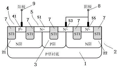
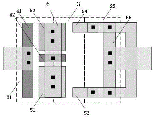
[0014] Such as figure 1 , figure 2 As shown, a high area efficiency diode-triggered thyristor based on two-dimensional design, including P-type substrate 1, N well 2, P well 3, P+ implant region 4, N+ implant region 5, metal 6, shallow trench isolation 7. The cathode 8 and the anode 9, the N well includes a first N well 21 and a second N well 22, the P+ injection region 4 includes a first P+ injection region 41 and a second P+ injection region 42, and the N+ injection region Region 5 includes a first N+ implantation region 51, a second N+ implantation region 52, a third N+ implantation region 53, a fourth N+ implantation region 54, and a fifth N+ implantation region 55, which are sequentially arranged on the P-type substrate 1 along the lateral direction. There are a first N well 21, a P well 3, and a second N well 22; the first N well 21 is provided with a first P+...


PUM


Abstract

The invention discloses high area efficiency diode triggered controllable silicon based on two-dimension design. The high area efficiency diode triggered controllable silicon based on the two-dimension design comprises a P-type substrate, N wells, a P well, P+ injection regions, N+ injection regions, metal, a shallow-trench isolation part, a cathode and an anode, wherein the N wells comprise a first N well and a second N well, the P+ injection region comprises a first P+ injection region and a second P+ injection region, the N+ injection regions comprise a first N+ injection region, a second N+ injection region, a third N+ injection region, a fourth N+ injection region and a fifth N+ injection region, and the first N well, the P well and the second N well are arranged on the P-type substrate in sequence along the transverse direction. According to the high area efficiency diode triggered controllable silicon based on the two-dimension design, a diode is embedded into the controllable silicon at a trigger stage, electric current flows mainly along the longitudinal direction of a device, thereby, well resistance in the longitudinal direction of the device is fully utilized, and compared with conventional diode triggered controllable silicon, the high area efficiency diode triggered controllable silicon based on the two-dimension design has the advantages that only a few of series diodes of the device are required so that high trigger voltage can be achieved, and the area efficiency is increased.

Description

technical field [0001] The invention relates to a high-area-efficiency diode-triggered thyristor based on a two-dimensional design, belonging to the technical field of integrated circuits. Background technique [0002] The phenomenon of electrostatic discharge (ESD) in nature poses a serious threat to the reliability of integrated circuits. In the industry, 37% of the failures of integrated circuit products are caused by electrostatic discharge. Moreover, with the increasing density of integrated circuits, on the one hand, due to the thinner and thinner silicon dioxide film (from micron to nanometer), the electrostatic pressure on the device is getting lower and lower; on the other hand, it is easy to generate and accumulate The extensive use of electrostatic materials such as plastics and rubbers greatly increases the probability of integrated circuits being damaged by electrostatic discharge. [0003] The modes of electrostatic discharge phenomena are generally divided i...

Claims


Application Information

Patent Timeline
Patent Type & Authority Applications(China)
IPC IPC(8): H01L29/06H01L29/74
CPCH01L29/06H01L29/74
Inventor 董树荣郭维钟雷曾杰王炜槐俞志辉
Owner HAINING BERNSTEIN BIOTECH CO LTD
Why Eureka
Try Eureka