

Gaas thin film grown on Si substrate and preparation method thereof
A substrate and thin film technology, applied in the field of GaAs thin film and its preparation, can solve the problems affecting the flatness of the surface of GaAs semiconductor devices, achieve the effect of simplifying the structure of the buffer layer and the epitaxial growth process, improving the quality of the crystal, and improving the flatness
- Summary
- Abstract
- Description
- Claims
- Application Information
AI Technical Summary
Problems solved by technology
Method used
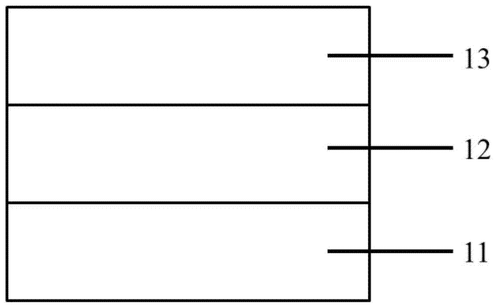
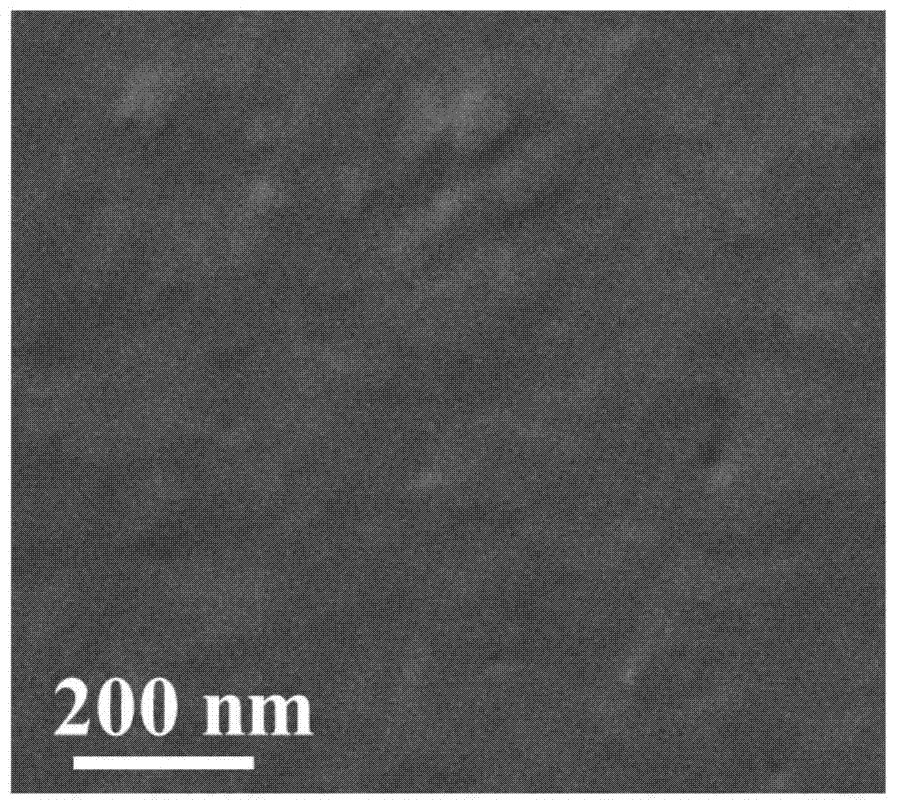
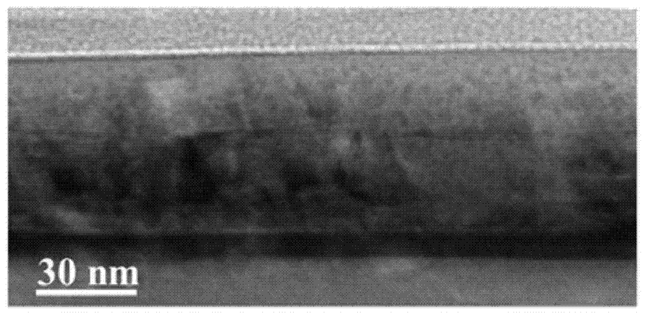
Image

Examples
Embodiment 1
[0036] The preparation method of the GaAs thin film grown on the Si substrate of the present embodiment comprises the following steps:
[0037] (1) Si substrate cleaning: After washing with acetone and deionized water, organic matter on the surface of the substrate is removed; the Si substrate is placed in HF:H 2 Ultrasound in O=1:10 solution for 1 minute, then rinse with deionized water to remove surface oxides and organic matter; dry the cleaned Si substrate with high-purity nitrogen;
[0038] (2) Si substrate pretreatment: After the Si substrate is cleaned, send it to the molecular beam epitaxy sampling chamber for pre-degassing for 15 minutes; then send it to the transfer chamber for degassing at 300°C for 2 hours, and send it to the growth chamber after degassing;
[0039] (3) Si substrate deoxidation film: after the Si substrate enters the growth chamber, the substrate temperature is raised to 950-1050 ° C, and the high-temperature baking is performed for 15-30 minutes t...
Embodiment 2
[0047] The preparation method of the GaAs thin film grown on the Si substrate of the present embodiment comprises the following steps:
[0048] (1) Si substrate cleaning: After washing with acetone and deionized water, organic matter on the surface of the substrate is removed; the Si substrate is placed in HF:H 2 Ultrasonic in O=1:10 solution for 10 minutes, then rinsed with deionized water to remove surface oxides and organic matter; the cleaned Si substrate was dried with high-purity nitrogen;
[0049] (2) Si substrate pretreatment: After the Si substrate is cleaned, send it to the molecular beam epitaxy sampling chamber for pre-degassing for 30 minutes; then send it to the transfer chamber for degassing at 400°C for 0.5 hours, and then send it to the growth chamber after degassing;
[0050] (3) Si substrate deoxidation film: after the Si substrate enters the growth chamber, the temperature of the substrate is raised to 1050 ° C, and the high temperature is baked for 30 minu...
PUM
| Property | Measurement | Unit |
|---|---|---|
| thickness | aaaaa | aaaaa |
Abstract
Description
Claims
Application Information