This helps you quickly interpret patents by identifying the three key elements:
Problems solved by technology
Method used
Benefits of technology
Problems solved by technology
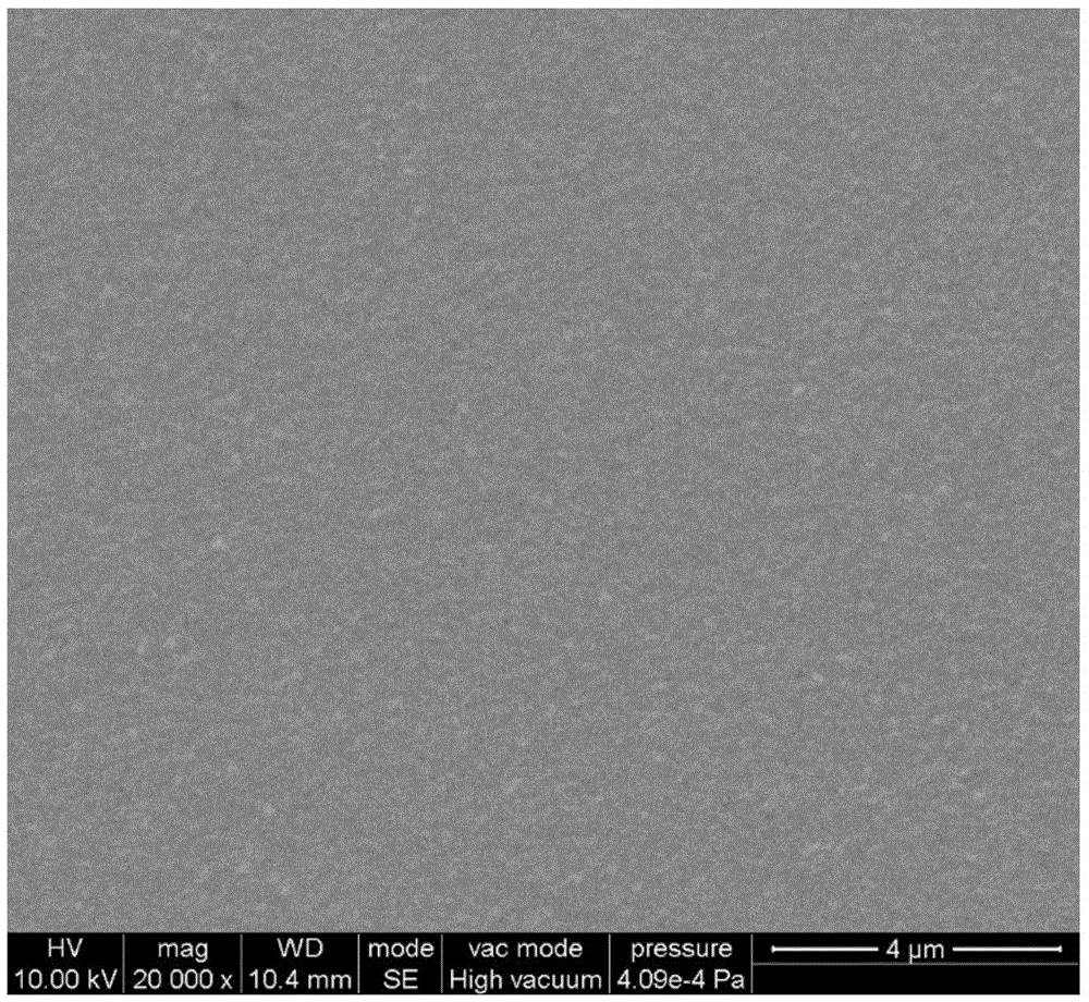
However, the growth steps of this graded structure buffer layer are often cumbersome, and it is difficult to precisely control the composition, thickness, and crystal quality of each layer of material, which affects the quality of the final GaAs film.
Method used
Image
Click on the blue label to locate the original text in one second.
Reading with bidirectional positioning of images and text.
Examples
Embodiment 1
[0048] The preparation method of the GaAs thin film grown on the Si substrate of the present embodiment comprises the following steps:
[0050] After washing with acetone and deionized water, the organic matter on the substrate surface was removed; the Si substrate was placed in HF:H 2 Ultrasound in O=1:10 solution for 1 minute, then rinse with deionized water to remove surface oxides and organic matter; dry the cleaned Si substrate with high-purity nitrogen;
[0052] After cleaning the Si(111) substrate, send it to the sample chamber for pre-degassing for 15 minutes; then send it to the transfer chamber for 0.5 hours at 300°C for degassing, and then send it to the growth chamber after degassing
[0076] After washing with acetone and deionized water, the organic matter on the substrate surface was removed; the Si substrate was placed in HF:H 2 Ultrasonic in O=1:10 solution for 10 minutes, then rinsed with deionized water to remove surface oxides and organic matter; the cleaned Si substrate was dried with high-purity nitrogen;
[0078] After the Si(111) substrate is cleaned, it is sent to the sample chamber for pre-degassing for 30 minutes; then sent to the transfer chamber for degassing at 400°C for 2 hours, and then sent to the growth chamber after degassing
[0080] After the Si(111) substrate enters the growth chamber, the temperature of the substrate is r...
PUM
Abstract
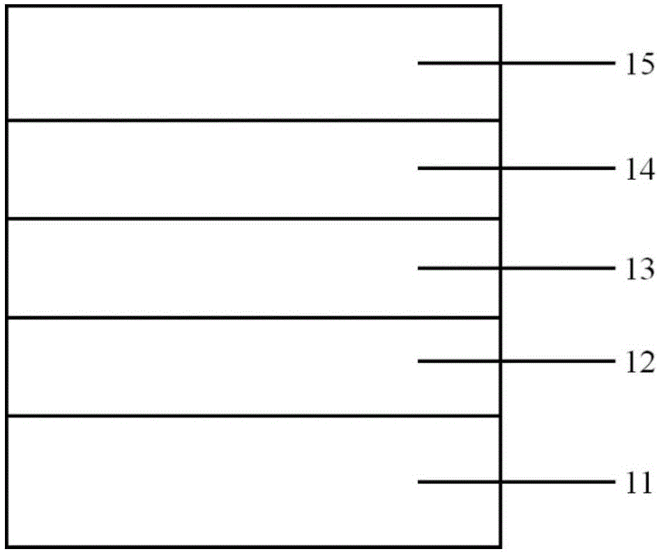
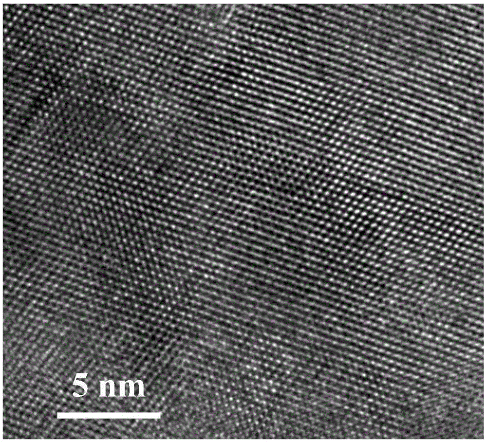
The invention discloses a preparation method of a GaAs film growing on a Si substrate. The method comprises the following steps: (1) cleaning the Si substrate (111); (2) pretreating the Si substrate (111); (3) deoxidizing the Si substrate (111); (4) growing a first In<x>Ga<1-x>As buffer layer; (5) annealing the first In<x>Ga<1-x>As buffer layer on situ; (6) growing a GaAs buffer layer; (7) annealing the GaAs buffer layer in situ; (8) growing a second In<x>Ga<1-x>As buffer layer; (9) annealing the second In<x>Ga<1-x>As buffer layer; and (10) growing a GaAs epitaxial film. The invention also discloses the GaAs film growing on the Si substrate. The obtained GaAs film is good in crystal quality and flat in surface, and has positive promoting significance to the preparation of semiconductors and the field of solar cells.
Description
technical field [0001] The invention relates to a GaAs thin film grown on a Si substrate, in particular to a GaAs thin film grown on a Si substrate and a preparation method thereof. Background technique [0002] Since Si has the advantages of mature technology, low price, high mechanical strength and easy large-scale size, the epitaxy of III-V semiconductor materials on Si, especially GaAs, is very attractive. If the epitaxial growth of high-quality GaAs materials on Si can be realized, the production cost of important semiconductor devices such as GaAs solar cells and optoelectronic detectors can be greatly reduced, and the combination of microelectronics and optoelectronics can be realized, which has broad application prospects. However, there are also some problems in epitaxial GaAs thin film on Si substrate. On the one hand, the lattice constant of Si is smaller than that of GaAs, and there is more than 4% lattice mismatch between them, which will cause a large number o...
Claims
Application Information
Patent Timeline
Application Date:The date an application was filed.
Publication Date:The date a patent or application was officially published.
First Publication Date:The earliest publication date of a patent with the same application number.
Issue Date:Publication date of the patent grant document.
PCT Entry Date:The Entry date of PCT National Phase.
Estimated Expiry Date:The statutory expiry date of a patent right according to the Patent Law, and it is the longest term of protection that the patent right can achieve without the termination of the patent right due to other reasons(Term extension factor has been taken into account ).
Invalid Date:Actual expiry date is based on effective date or publication date of legal transaction data of invalid patent.

