
GaAs thin film growing on Si substrate and method for preparing same

A substrate and thin film technology, applied in the field of GaAs thin films and their preparation, can solve problems affecting the surface flatness of GaAs semiconductor devices, etc., and achieve a simplified buffer layer structure and an epitaxial growth process, the technical means are simple and feasible, and the epitaxial growth process is simplified Effect

Active Publication Date: 2015-08-12
SOUTH CHINA UNIV OF TECH
View PDF4 Cites 7 Cited by
  • Summary
  • Abstract
  • Description
  • Claims
  • Application Information

AI Technical Summary

Problems solved by technology

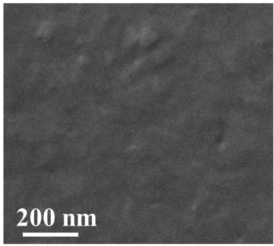
[0004] On the other hand, because {111} is the twin plane in the face-centered cubic compound and the special reconstruction of Ga on the Si(111) plane, a large number of twin crystals will be generated in the epitaxial GaAs film on Si(111) , forming a large number of pyramid-shaped protrusions on the surface of the film, which seriously affects the surface flatness of GaAs semiconductor devices

Method used


Image

  • GaAs thin film growing on Si substrate and method for preparing same
  • GaAs thin film growing on Si substrate and method for preparing same
  • GaAs thin film growing on Si substrate and method for preparing same

Examples


Embodiment 1

[0036] The preparation method of the GaAs thin film grown on the Si substrate of the present embodiment comprises the following steps:

[0037] (1) Si substrate cleaning: After washing with acetone and deionized water, organic matter on the surface of the substrate is removed; the Si substrate is placed in HF:H 2 Ultrasound in O=1:10 solution for 1 minute, then rinse with deionized water to remove surface oxides and organic matter; dry the cleaned Si substrate with high-purity nitrogen;

[0038] (2) Si substrate pretreatment: After the Si substrate is cleaned, send it to the molecular beam epitaxy sampling chamber for pre-degassing for 15 minutes; then send it to the transfer chamber for degassing at 300°C for 2 hours, and send it to the growth chamber after degassing;

[0039] (3) Deoxidation film on Si substrate: After Si substrate enters the growth chamber, raise the substrate temperature to 950-1050°C, bake at high temperature for 15-30 minutes, and remove the oxide film l...

Embodiment 2

[0047] The preparation method of the GaAs thin film grown on the Si substrate of the present embodiment comprises the following steps:

[0048] (1) Si substrate cleaning: After washing with acetone and deionized water, organic matter on the surface of the substrate is removed; the Si substrate is placed in HF:H 2 Ultrasonic in O=1:10 solution for 10 minutes, then rinsed with deionized water to remove surface oxides and organic matter; the cleaned Si substrate was dried with high-purity nitrogen;

[0049] (2) Si substrate pretreatment: After the Si substrate is cleaned, send it to the molecular beam epitaxy sampling chamber for pre-degassing for 30 minutes; then send it to the transfer chamber for degassing at 400°C for 0.5 hours, and then send it to the growth chamber after degassing;

[0050] (3) Si substrate deoxidation film: after the Si substrate enters the growth chamber, the temperature of the substrate is raised to 1050 ° C, and the high temperature is baked for 30 minu...


PUM

PropertyMeasurementUnit
thicknessaaaaaaaaaa

Abstract

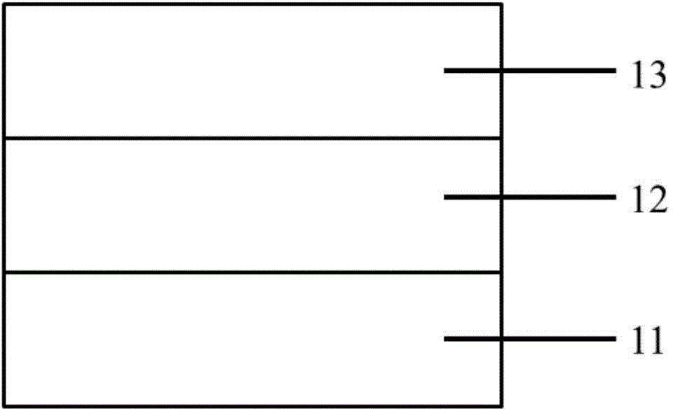
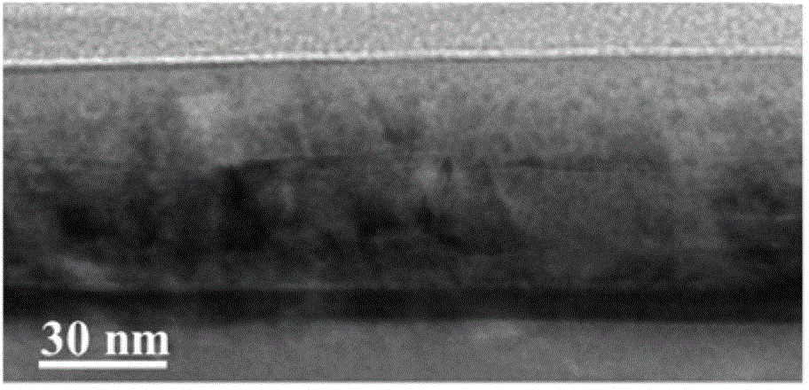
The present invention discloses a GaAs thin film growing on a Si substrate and a method for preparing the same. The method comprises the steps of (1) cleaning the Si substrate; (2) pre-processing the Si substrate; (4) growing a buffer layer, namely growing an InxGa(1-x)As buffer layer on the surface of the Si substrate after the processing of the step (3) at the growth temperature of 350-500 DEG C, wherein the 0.08<x<0.12; and (5) growing the GaAs thin film, namely growing the GaAs thin film at the growth temperature of 500-580 DEG C. The present invention also discloses the GaAs thin film growing on the Si substrate. The GaAs thin film growing on the Si substrate comprises the Si substrate, the InxGa(1-x)As buffer layer and the GaAs thin film which are laminated orderly. The preparation method of the present invention is simple, enables the structure of the buffer layer and an epitaxial growth technology to be simplified greatly, and obtains the GaAs epitaxial thin film which is good in surface appearance and low in residual stress.

Description

technical field [0001] The invention relates to a GaAs film and a preparation method thereof, in particular to a GaAs film grown on a Si substrate and a preparation method thereof. Background technique [0002] Since Si has the advantages of mature technology, low price and easy large-scale size, epitaxial III-V semiconductor materials on silicon, especially GaAs, are very attractive. At present, researchers have successfully epitaxially grown GaAs-based lasers, high-efficiency solar cells and other optoelectronic devices with special optoelectronic properties on Si substrates. Usually, GaAs semiconductor devices are prepared by epitaxial growth on the Si(100) surface. However, there are two problems in the epitaxial growth of GaAs on Si(100). On the one hand, due to the monoatomic step surface of Si(100), there are a large number of reverse domain defects in the epitaxial GaAs film directly on the Si(100) substrate. On the other hand, because Si(100) has a large surface ...

Claims


Application Information

Patent Timeline
Patent Type & Authority Applications(China)
IPC IPC(8): H01L21/02H01L31/18H01L31/0304H01S5/323H01S5/343
CPCH01L21/02381H01L21/02463H01L21/02546H01L31/03046H01L31/1844H01L31/1852H01S5/323H01S5/343Y02P70/50
Inventor 李国强温雷高芳亮张曙光李景灵管云芳
Owner SOUTH CHINA UNIV OF TECH
Learn More