
GaAs substrate-based gallium oxide thin film and growing method thereof

A gallium oxide and substrate technology, applied in the field of microelectronics, can solve the problems of poor surface morphology and small grain size of Ga2O3 thin films

Inactive Publication Date: 2015-10-07
XIDIAN UNIV
View PDF3 Cites 13 Cited by
  • Summary
  • Abstract
  • Description
  • Claims
  • Application Information

AI Technical Summary

Problems solved by technology

[0006] However, at present, Ga2O3 thin films are deposited by PLD using a single growth method, that is, the same process parameters are used during the growth process, including oxygen pressure, laser energy, substrate temperature, etc., so that PLD technology can be used on GaAs substrates. Poor surface morphology and small grain size of Ga2O3 films obtained by heteroepitaxial

Method used


Image

  • GaAs substrate-based gallium oxide thin film and growing method thereof
  • GaAs substrate-based gallium oxide thin film and growing method thereof

Examples


Embodiment 1

[0028] Example 1, making a gallium oxide film with a buffer layer thickness of 6 nm.

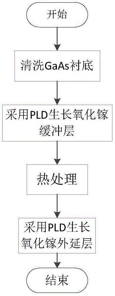
[0029] Step 1, cleaning the GaAs substrate.

[0030] (1.1) ultrasonically clean the GaAs substrate with toluene, acetone, ethanol and deionized water for 5 minutes in sequence;

[0031] (1.2) Soak the GaAs substrate in a mixed solution of sulfuric acid, hydrogen peroxide and water at a ratio of 5:1:1 at 60-70°C for 1 min;

[0032] (1.3) Rinse the GaAs substrate with deionized water and dry it with N2.

[0033] Step 2, growing a gallium oxide buffer layer with a thickness of 6 nm.

[0034] (2.1) Put the cleaned GaAs substrate into the pulsed laser deposition PLD chamber, and pump the vacuum degree of the pulsed laser deposition PLD chamber to 10 -6 mbar, the distance between the substrate and the gallium oxide target is adjusted to 50mm, and the speed of the target is kept at 30rpm;

[0035] (2.2) Heat the GaAs substrate to 700°C, adjust the oxygen partial pressure in the pulsed laser dep...

Embodiment 2

[0042] Example 2, making a gallium oxide thin film with a buffer layer thickness of 12nm.

[0043] The first step is to clean the GaAs substrate.

[0044] This step is the same as Step 1 of Example 1.

[0045] In the second step, a gallium oxide buffer layer with a thickness of 12nm is grown.

[0046] 2.1) Put the cleaned GaAs substrate into the pulsed laser deposition PLD chamber, and pump the vacuum degree of the pulsed laser deposition PLD chamber to 10 -6 mbar, the distance between the substrate and the gallium oxide target is adjusted to 50mm, and the speed of the target is kept at 30rpm;

[0047] 2.2) Heat the GaAs substrate to 625°C, adjust the oxygen partial pressure in the pulsed laser deposition PLD chamber to 0.06mbar, set the laser energy to 310mJ, the laser frequency to 3Hz, and the number of pulses to 1500 to grow the Ga2O3 buffer layer;

[0048] 2.3) After the growth of the buffer layer is completed, the pulsed laser deposition PLD chamber is filled with 200 ...

Embodiment 3

[0059] Example 3, making a gallium oxide thin film with a buffer layer thickness of 10 nm.

[0060] Step A, cleaning the GaAs substrate.

[0061] The implementation of this step is the same as step 1 in Embodiment 1.

[0062] Step B, growing a gallium oxide buffer layer with a thickness of 10 nm.

[0063] (B1) Put the cleaned GaAs substrate into the pulsed laser deposition PLD chamber, and pump the vacuum degree of the pulsed laser deposition PLD chamber to 10 -6 mbar, the distance between the substrate and the gallium oxide target is adjusted to 50mm, and the speed of the target is kept at 30rpm;

[0064] (B2) Heating the substrate to 650°C, adjusting the oxygen partial pressure in the pulsed laser deposition PLD chamber to 0.05mbar, setting the laser energy to 340mJ, the laser frequency to 4Hz, and the number of pulses to 1200 to grow a Ga2O3 buffer layer;

[0065] (B3) After the growth of the buffer layer is completed, 200 mbar of oxygen is filled into the pulsed laser d...


PUM

PropertyMeasurementUnit
Thicknessaaaaaaaaaa
Thicknessaaaaaaaaaa
Thicknessaaaaaaaaaa

Abstract

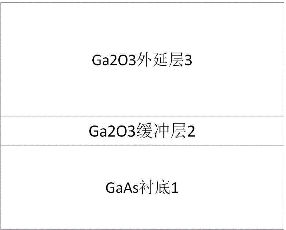
The invention discloses a GaAs substrate-based gallium oxide thin film and a growing method thereof, and mainly solves the problems of poor surface appearance and small grain size of an existing gallium oxide thin film. The gallium oxide thin film comprises a GaAs substrate (1) and a gallium oxide epitaxial layer (3), and is characterized in that a gallium oxide buffer layer (2) of 6 to 12 nm is arranged between the GaAs substrate (1) and the gallium oxide epitaxial layer (3), and the crystal quality of the gallium oxide buffer layer is improved by utilizing thermal annealing. The surface roughness of a Ga2O3 thin film is reduced, the surface appearance of the Ga2O3 thin film is improved, and the Ga2O3 grain size is increased; the GaAs substrate-based gallium oxide thin film and the growing method can be used for making semiconductor power devices.

Description

technical field [0001] The invention belongs to the technical field of microelectronics, and relates to a method for growing semiconductor materials, in particular to a Ga2O3 thin film manufacturing method, which can be used for manufacturing semiconductor power devices. Background technique [0002] In recent years, the third-generation semiconductors represented by SiC and GaN have been widely used due to their characteristics such as large band gap, high breakdown electric field, high thermal conductivity, high saturation electron velocity and high concentration of two-dimensional electron gas at the heterojunction interface. focus on. Although the third-generation semiconductor materials and devices have made significant progress and have entered the stage of practical application, their wide-ranging applications are still limited due to many defects in SiC and GaN materials. For this reason, on the basis of the growth of SiC and GaN materials, device manufacturing and ...

Claims


Application Information

Patent Timeline
IPC IPC(8): C23C14/02C23C14/28C23C14/08H01L21/20
Inventor 冯倩李付国代波谢文林徐通郝跃
Owner XIDIAN UNIV
Learn More