Photoelectric material adjustable absorption enhancing layer based on graphene surface plasmon

A graphene surface and optoelectronic material technology, applied in circuits, electrical components, semiconductor devices, etc., can solve problems such as high cost, incompatibility of manufacturing process, and application limitations, so as to improve overall performance, realize cheap mass production, and source rich effect

Inactive Publication Date: 2015-08-19
NAT UNIV OF DEFENSE TECH
View PDF2 Cites 33 Cited by
  • Summary
  • Abstract
  • Description
  • Claims
  • Application Information

AI Technical Summary

Problems solved by technology

However, the traditional surface plasmon materials are mainly precious metals such as gold and silver. These materials are expensive and incompatible with the traditional semiconductor material manufacturing process, which makes their application in optoelectronic devices such as solar cells and photodetectors restricted. very restrictive

Method used


Image

  • Photoelectric material adjustable absorption enhancing layer based on graphene surface plasmon
  • Photoelectric material adjustable absorption enhancing layer based on graphene surface plasmon
  • Photoelectric material adjustable absorption enhancing layer based on graphene surface plasmon

Examples


Embodiment Construction

[0031] The specific embodiments of the present invention will be further introduced below in conjunction with the accompanying drawings.

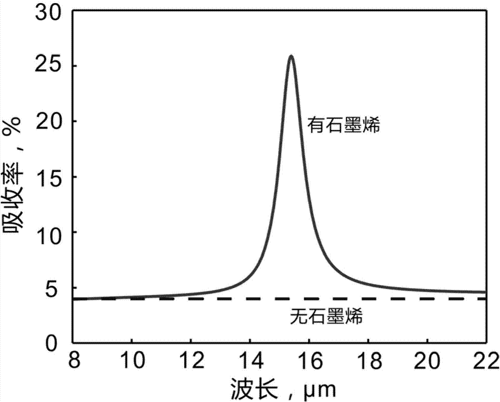
[0032] The invention utilizes the surface plasmon resonance characteristics of the graphene micro-nano structure to enhance and control the absorption of light by the photoelectric material.

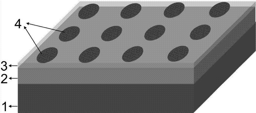
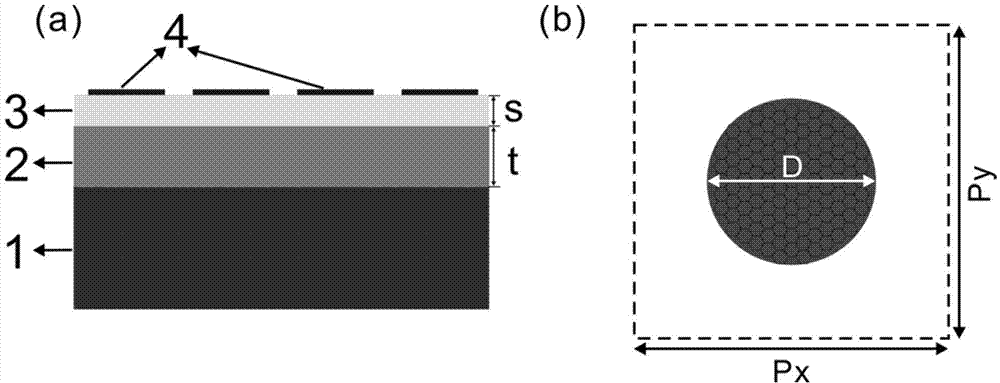
[0033] figure 1 Shown is the graphene micro-nano structure-based photoelectric material tunable absorption enhancement layer and the structural composition schematic diagram applied to enhance the absorption of the photoelectric material (Example 1). In the figure, 1 is a substrate, 2 is a photoelectric absorption material, 3 is a dielectric spacer layer, and 4 is an absorption enhancement layer. The absorption enhancement layer is a graphene micro-nano structure. The substrate 1 and the photoelectric absorption material 2 are common photoelectric It is an indispensable part of the photoelectric energy conversion structural unit in devices (such as solar c...


PUM

PropertyMeasurementUnit
thicknessaaaaaaaaaa
thicknessaaaaaaaaaa
thicknessaaaaaaaaaa

Abstract

The invention belongs to the field of photoelectric technology, and specifically relates to a photoelectric material adjustable absorption enhancing layer based on graphene surface plasmon. Graphene forming the enhancing layer is a thin film formed by single-layer graphene and having micro-nano scale structural features, graphene is doped to a certain concentration, and the Fermi level Ef of the graphene is larger than 0.1eV or smaller than -0.1eV, so that the graphene becomes a surface plasmon material; and the micro-nano structure is used for realizing wave-vector matching between incident light and a graphene surface plasmon mode, and under irradiation of the incident light, the doped graphene micro-nano structure generates surface plasmon, thereby realizing a local area of focusing. The absorption enhancing layer is applied to the upper side of photoelectric material used by photoelectric devices such as a solar cell and a photoelectric detector, can improve the absorption efficiency of the photoelectric material, and can realize active regulation and control of absorption characteristics of the photoelectric material, thereby expanding application of the photoelectric material in fields of spectrum-adjustable selective detection and the like.

Description

Technical field [0001] The invention belongs to the field of optoelectronic technology, and in particular relates to a photoelectric material tunable absorption enhancement layer based on graphene surface plasmons. Background technique [0002] The absorption performance of optoelectronic materials has an important influence on the performance of optoelectronic devices. Photovoltaic devices, photodetectors, and other optoelectronic devices rely on optoelectronic materials to convert the absorbed light into electrical energy or electrical signals to achieve their functions. In the case of a certain conversion efficiency, the more light absorbed, the greater the intensity of the generated electric energy or electrical signal, and the higher the overall efficiency of the optoelectronic device. [0003] In some optoelectronic devices, such as thin-film solar cells, they are limited by the carrier life of optoelectronic materials, or in order to reduce the use of materials and reduce c...

Claims


Application Information

Patent Timeline
Patent Type & Authority Applications(China)
IPC IPC(8): H01L31/0232
CPCH01L31/02327
Inventor 张检发朱志宏袁晓东秦石乔
Owner NAT UNIV OF DEFENSE TECH
Why Eureka
Try Eureka